Logic Gate and Binary Adder Experimentation Board
Circuit Documentation
Summary
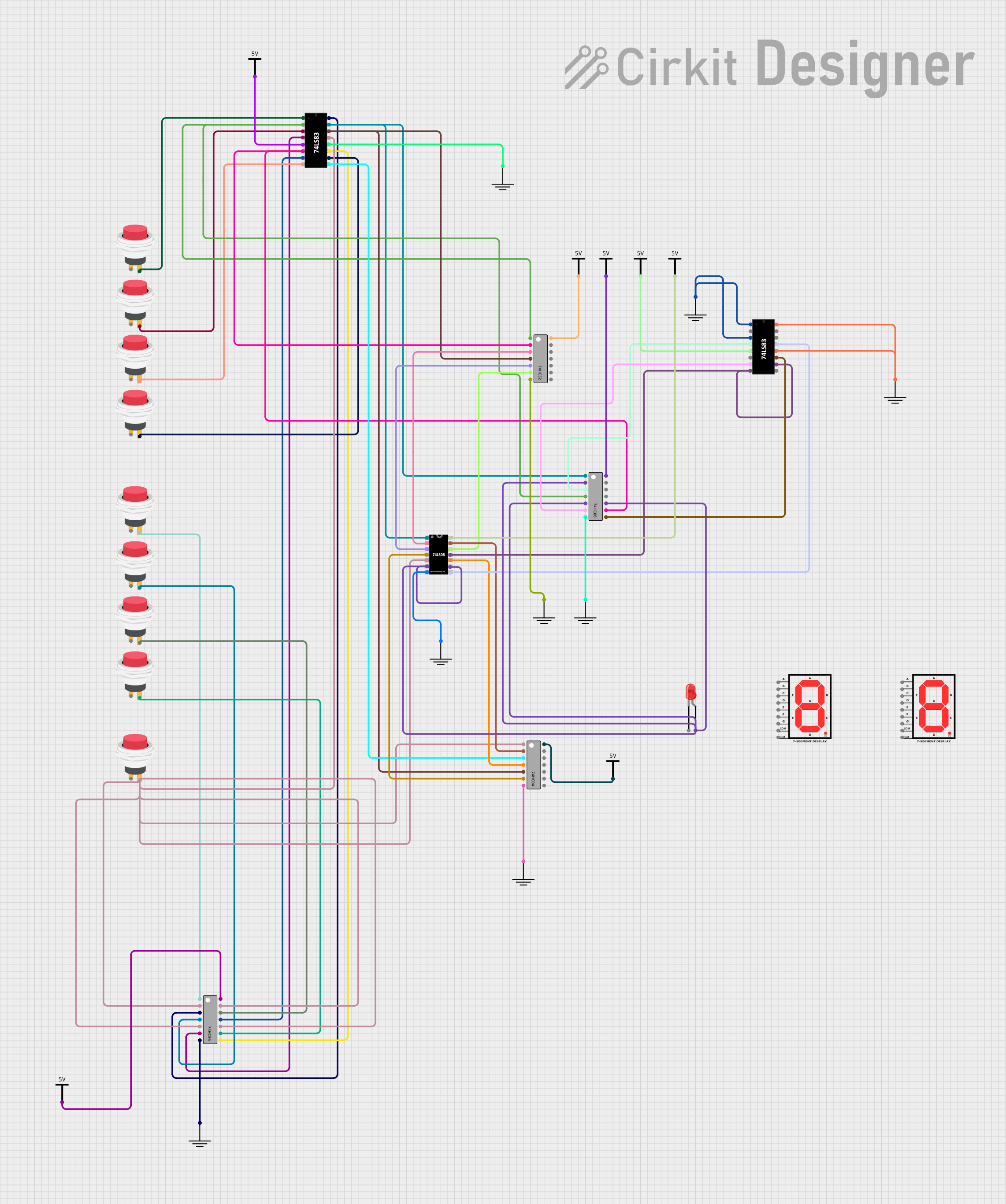
This document provides a detailed overview of a digital logic circuit. The circuit comprises a combination of logic gates, switches, a binary adder, and display elements. The logic gates include inverters (74HC04), XOR gates (74HC86), OR gates (74HC32), and AND gates (IC 7408). The binary adder is represented by two instances of IC 7483, and the display elements are two 7-segment displays. Additionally, the circuit includes multiple push switches and LEDs for input and output visualization, respectively. Power supply connections are made through Vcc and GND components.
Component List
- 74HC04: Hex inverter chip, containing six inverters.
- 74HC86: Quad 2-input XOR gate chip, containing four XOR gates.
- 74HC32: Quad 2-input OR gate chip, containing four OR gates.
- IC 7408: Quad 2-input AND gate chip, containing four AND gates.
- IC 7483: 4-bit binary full adder, capable of adding two 4-bit numbers and outputting the sum and carry-out.
- 7segment on: 7-segment LED display for numerical output.
- 2Pin Push Switch: Pushbutton switch used for providing binary input.
- LED: Two Pin (red): Red LED used for indicating binary output or status.
- Vcc: Power supply component representing the positive voltage supply.
- GND: Ground component representing the circuit common ground.
Wiring Details
74HC04 (Hex Inverter)
- A1, A2, A3: Input pins for inverters.
- Y1, Y2, Y3: Output pins for inverters.
- GND: Connected to the circuit common ground.
- VCC: Connected to the positive voltage supply.
74HC86 (Quad 2-input XOR Gate)
- A1, A2, A3, A4: First input pins for XOR gates.
- B1, B2, B3, B4: Second input pins for XOR gates.
- Y1, Y2, Y3, Y4: Output pins for XOR gates.
- GND: Connected to the circuit common ground.
- VCC: Connected to the positive voltage supply.
74HC32 (Quad 2-input OR Gate)
- A1, A2, A3, A4: First input pins for OR gates.
- B1, B2, B3, B4: Second input pins for OR gates.
- Y1, Y2, Y3, Y4: Output pins for OR gates.
- GND: Connected to the circuit common ground.
- VCC: Connected to the positive voltage supply.
IC 7408 (Quad 2-input AND Gate)
- A1, A2, A3, A4: First input pins for AND gates.
- B1, B2, B3, B4: Second input pins for AND gates.
- Y1, Y2, Y3, Y4: Output pins for AND gates.
- GND: Connected to the circuit common ground.
- VCC: Connected to the positive voltage supply.
IC 7483 (4-bit Binary Full Adder)
- A1, A2, A3, A4: First 4-bit input for addition.
- B1, B2, B3, B4: Second 4-bit input for addition.
- S1, S2, S3, S4: 4-bit sum output.
- C0: Carry-in input.
- C4: Carry-out output.
- GND: Connected to the circuit common ground.
- VCC: Connected to the positive voltage supply.
7segment on (7-Segment LED Display)
- A, B, C, D, E, F, G: Segment control inputs.
- COM: Common pin for the display.
- dot: Control input for the decimal point.
2Pin Push Switch
- Input +: Input pin for the switch.
- Output +: Output pin for the switch.
LED: Two Pin (red)
- cathode: Cathode pin of the LED.
- anode: Anode pin of the LED.
Vcc
- Vcc: Positive voltage supply pin.
GND
- GND: Ground pin.
Documented Code
No microcontroller code was provided for this circuit. If any embedded code is required for microcontrollers in future iterations of the circuit, it will be documented in this section.