How to Use CD4081 Quad Input AND Gate IC: Examples, Pinouts, and Specs
Introduction
The CD4081 is a quad 2-input AND gate integrated circuit (IC) designed to perform logical AND operations. It contains four independent AND gates, each with two inputs and one output. This IC is widely used in digital circuits for implementing logic functions, such as signal control, data processing, and decision-making in embedded systems.
Explore Projects Built with CD4081 Quad Input AND Gate IC

Explore Projects Built with CD4081 Quad Input AND Gate IC
Common Applications and Use Cases
- Digital logic circuits
- Signal gating and control
- Data routing and processing
- Embedded systems and microcontroller projects
- Timing and synchronization circuits
Technical Specifications
The CD4081 IC is built using CMOS technology, which ensures low power consumption and high noise immunity. Below are the key technical details:
| Parameter | Value |
|---|---|
| Supply Voltage (VDD) | 3V to 15V |
| Input Voltage Range | 0V to VDD |
| Output Voltage Range | 0V to VDD |
| Maximum Input Current | ±10 µA |
| Maximum Output Current | ±10 mA |
| Propagation Delay | 60 ns (typical at 5V) |
| Power Dissipation | 500 mW (maximum) |
| Operating Temperature Range | -55°C to +125°C |
| Package Types | DIP-14, SOIC-14, TSSOP-14 |
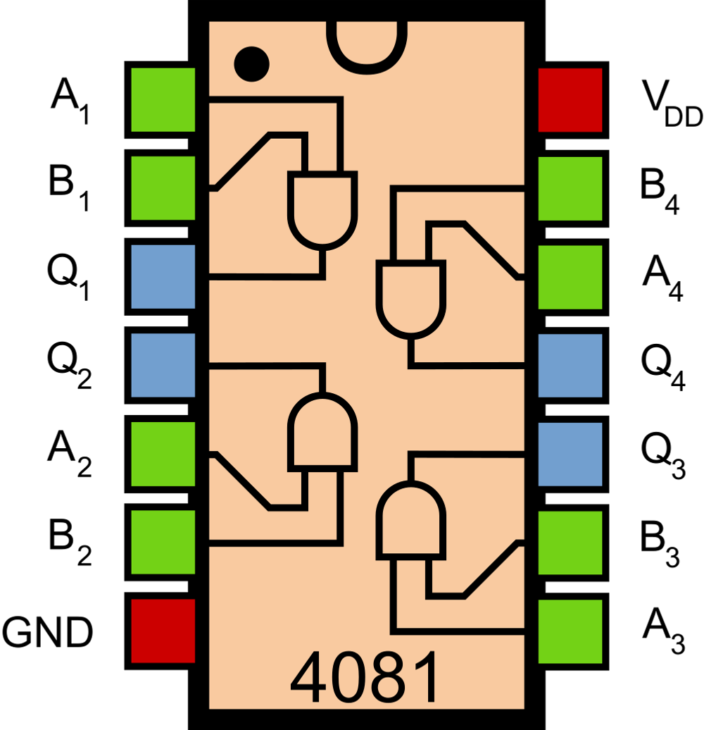
Pin Configuration and Descriptions
The CD4081 IC comes in a 14-pin package. Below is the pinout and description:
| Pin Number | Pin Name | Description |
|---|---|---|
| 1 | A1 | Input 1 of Gate 1 |
| 2 | B1 | Input 2 of Gate 1 |
| 3 | Y1 | Output of Gate 1 |
| 4 | A2 | Input 1 of Gate 2 |
| 5 | B2 | Input 2 of Gate 2 |
| 6 | Y2 | Output of Gate 2 |
| 7 | GND | Ground (0V) |
| 8 | Y3 | Output of Gate 3 |
| 9 | A3 | Input 1 of Gate 3 |
| 10 | B3 | Input 2 of Gate 3 |
| 11 | Y4 | Output of Gate 4 |
| 12 | A4 | Input 1 of Gate 4 |
| 13 | B4 | Input 2 of Gate 4 |
| 14 | VDD | Positive Supply Voltage |
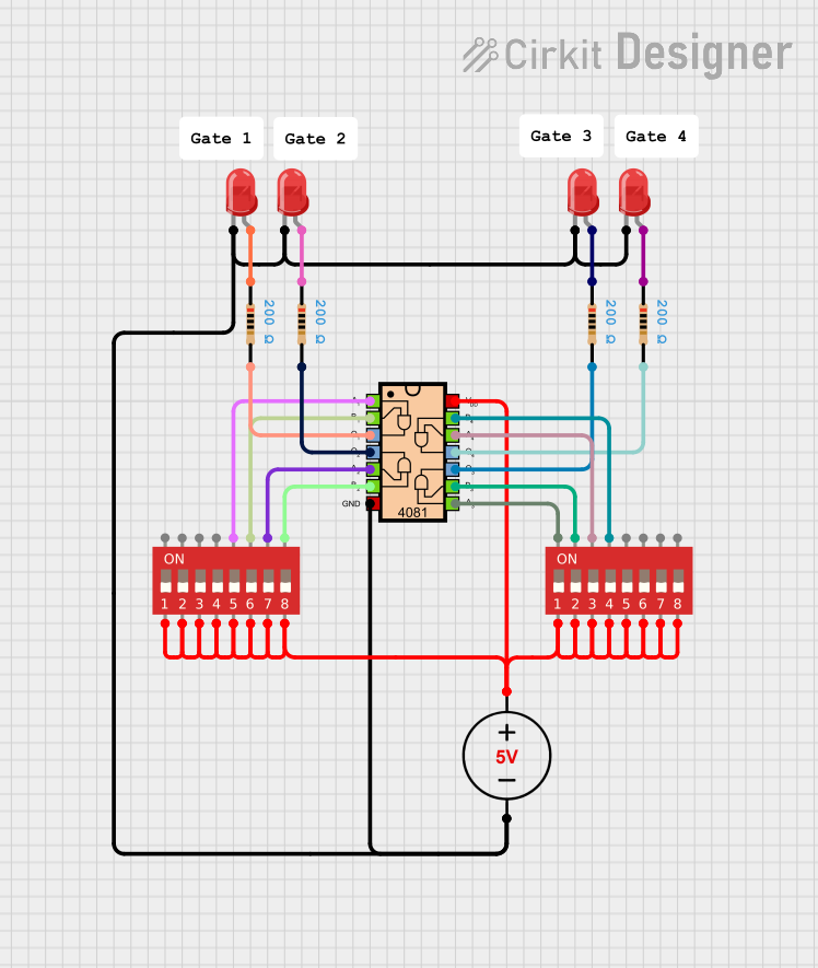
Usage Instructions
How to Use the CD4081 in a Circuit
- Power Supply: Connect the VDD pin (Pin 14) to the positive supply voltage (3V to 15V) and the GND pin (Pin 7) to ground.
- Inputs: Provide the input signals to the respective input pins (A1, B1, A2, B2, etc.).
- Outputs: The output pins (Y1, Y2, Y3, Y4) will provide the logical AND result of the corresponding input pairs.
- Pull-Down Resistors: If the inputs are left floating, use pull-down resistors to avoid undefined behavior.
Important Considerations and Best Practices
- Ensure the supply voltage does not exceed the maximum rating of 15V to prevent damage.
- Avoid leaving input pins floating; always connect them to a defined logic level (HIGH or LOW).
- Use decoupling capacitors (e.g., 0.1 µF) near the VDD pin to reduce noise and improve stability.
- Verify the propagation delay in timing-critical applications.
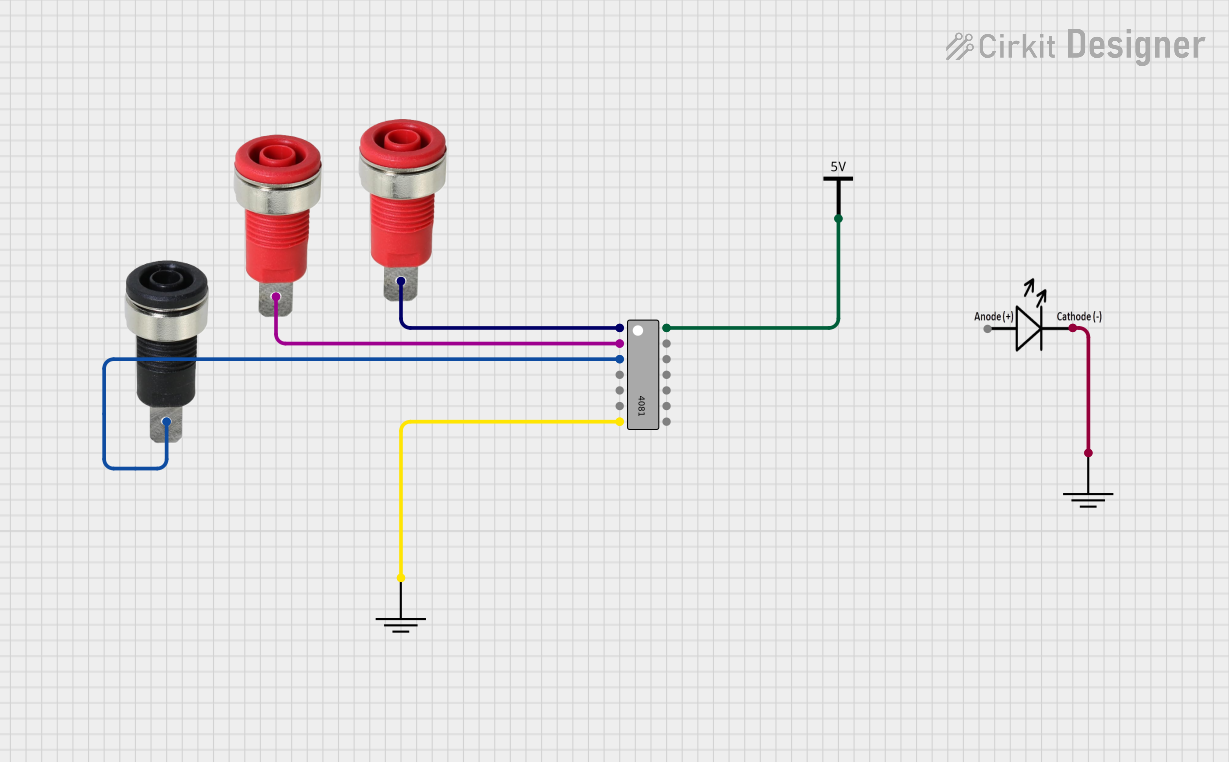
Example: Connecting CD4081 to an Arduino UNO
The CD4081 can be used with an Arduino UNO to perform logical AND operations. Below is an example circuit and code:
Circuit Setup
- Connect the VDD pin (Pin 14) to the Arduino's 5V pin and the GND pin (Pin 7) to the Arduino's GND.
- Connect two digital output pins of the Arduino (e.g., D2 and D3) to the inputs of one AND gate (e.g., A1 and B1).
- Connect the output of the AND gate (e.g., Y1) to another digital input pin of the Arduino (e.g., D4).
Arduino Code
// CD4081 AND Gate Example with Arduino UNO
// This code demonstrates how to use the CD4081 to perform a logical AND operation.

const int input1 = 2;  // Arduino pin connected to A1 (Input 1 of Gate 1)
const int input2 = 3;  // Arduino pin connected to B1 (Input 2 of Gate 1)
const int output = 4;  // Arduino pin connected to Y1 (Output of Gate 1)

void setup() {
  pinMode(input1, OUTPUT);  // Set input1 as an output pin
  pinMode(input2, OUTPUT);  // Set input2 as an output pin
  pinMode(output, INPUT);   // Set output as an input pin

  Serial.begin(9600);       // Initialize serial communication
}

void loop() {
  digitalWrite(input1, HIGH);  // Set Input 1 to HIGH
  digitalWrite(input2, HIGH);  // Set Input 2 to HIGH

  // Read the output of the AND gate
  int andOutput = digitalRead(output);

  // Print the result to the Serial Monitor
  Serial.print("AND Gate Output: ");
  Serial.println(andOutput);

  delay(1000);  // Wait for 1 second
}
Troubleshooting and FAQs
Common Issues and Solutions
No Output Signal:
- Ensure the power supply is connected properly to the VDD and GND pins.
- Verify that the input signals are at valid logic levels (0V or VDD).
Incorrect Output:
- Check for floating input pins and use pull-down resistors if necessary.
- Verify the connections and ensure the correct pins are used for inputs and outputs.
Overheating:
- Ensure the supply voltage does not exceed the maximum rating of 15V.
- Avoid drawing excessive current from the output pins.
FAQs
Q1: Can the CD4081 operate at 3.3V?
Yes, the CD4081 can operate at a supply voltage as low as 3V, making it compatible with 3.3V systems.
Q2: What happens if one input is HIGH and the other is LOW?
The output of the AND gate will be LOW, as both inputs must be HIGH for the output to be HIGH.
Q3: Can I use the CD4081 with other logic families?
Yes, but ensure proper voltage level matching between the CD4081 and other components in the circuit.
Q4: How many gates can I use simultaneously?
All four gates in the CD4081 can be used independently and simultaneously.