
How to Use SHIFT REGISTER: Examples, Pinouts, and Specs
 Design with SHIFT REGISTER in Cirkit Designer
Introduction
The 74*595 is an 8-bit serial-in, parallel-out shift register with a storage register and tri-state outputs. It is widely used in digital electronics to expand the number of output pins available on a microcontroller or microprocessor. By cascading multiple shift registers, users can control a large number of outputs using only a few pins.
Explore Projects Built with SHIFT REGISTER
 Open Project in Cirkit Designer
 Open Project in Cirkit Designer
 Open Project in Cirkit Designer
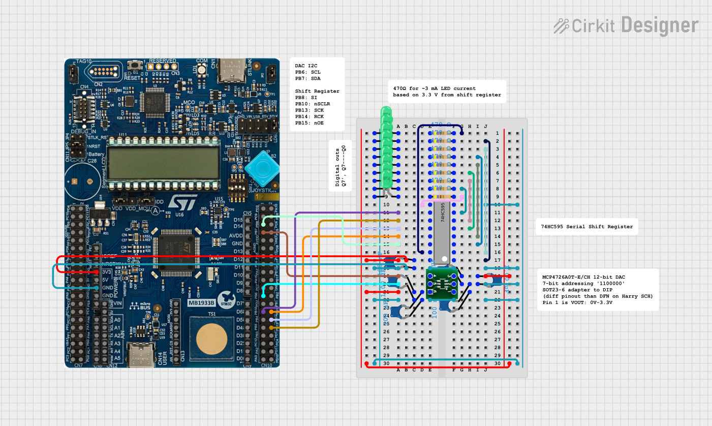 Open Project in Cirkit Designer
Explore Projects Built with SHIFT REGISTER
Open Project in Cirkit DesignerOpen Project in Cirkit DesignerOpen Project in Cirkit DesignerOpen Project in Cirkit DesignerCommon Applications and Use Cases
- Driving LED arrays or 7-segment displays
- Expanding GPIO pins on microcontrollers
- Controlling relays or other digital outputs
- Data storage and transfer in digital circuits
- Multiplexing and demultiplexing signals
Technical Specifications
The 74*595 shift register is a versatile component with the following key specifications:
| Parameter | Value |
|---|---|
| Supply Voltage (Vcc) | 2V to 6V |
| Input Voltage (VI) | 0V to Vcc |
| Output Current (IOH/IOL) | ±6mA (max) |
| Maximum Clock Frequency | 25 MHz (at 5V) |
| Operating Temperature | -40°C to +125°C |
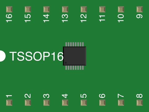
| Package Types | DIP-16, SOIC-16, TSSOP-16 |
Pin Configuration and Descriptions
The 74*595 has 16 pins, as described in the table below:
| Pin Number | Pin Name | Description |
|---|---|---|
| 1 | Q1 | Parallel output pin 1 |
| 2 | Q2 | Parallel output pin 2 |
| 3 | Q3 | Parallel output pin 3 |
| 4 | Q4 | Parallel output pin 4 |
| 5 | Q5 | Parallel output pin 5 |
| 6 | Q6 | Parallel output pin 6 |
| 7 | Q7 | Parallel output pin 7 |
| 8 | GND | Ground (0V) |
| 9 | Q7' | Serial data output for cascading additional shift registers |
| 10 | MR | Master reset (active low) |
| 11 | SH_CP | Shift register clock input |
| 12 | ST_CP | Storage register clock input (latch pin) |
| 13 | OE | Output enable (active low) |
| 14 | DS | Serial data input |
| 15 | Q0 | Parallel output pin 0 |
| 16 | Vcc | Positive supply voltage |
Usage Instructions
The 74*595 shift register is easy to use in digital circuits. Below are the steps and considerations for using it effectively:
Connecting the 74*595
- Power Supply: Connect the Vcc pin to a 5V or 3.3V power source (depending on your system) and the GND pin to ground.
- Data Input: Connect the DS pin to the data source (e.g., a microcontroller pin).
- Clock Pins:
- Connect the SH_CP pin to the clock signal for shifting data into the register.
- Connect the ST_CP pin to the clock signal for latching the data to the output pins.
- Output Enable: Connect the OE pin to ground to enable the outputs. If you want to disable the outputs, connect OE to Vcc.
- Outputs: Use the Q0–Q7 pins to drive your desired load (e.g., LEDs, relays).
- Cascading: To cascade multiple shift registers, connect the Q7' pin of the first register to the DS pin of the next register.
Example Circuit with Arduino UNO
Below is an example of how to connect and control a 74*595 shift register with an Arduino UNO to drive 8 LEDs:
Circuit Connections
- Connect the 74*595 Vcc pin to the Arduino 5V pin and GND to Arduino GND.
- Connect the DS pin to Arduino pin 11.
- Connect the SH_CP pin to Arduino pin 12.
- Connect the ST_CP pin to Arduino pin 8.
- Connect the OE pin to GND.
- Connect LEDs to Q0–Q7 through 220-ohm resistors.
Arduino Code Example
// Define pins for the 74*595 shift register
const int dataPin = 11;  // DS pin
const int clockPin = 12; // SH_CP pin
const int latchPin = 8;  // ST_CP pin

void setup() {
  // Set pins as outputs
  pinMode(dataPin, OUTPUT);
  pinMode(clockPin, OUTPUT);
  pinMode(latchPin, OUTPUT);
}

void loop() {
  // Example: Turn on LEDs one by one
  for (int i = 0; i < 256; i++) {
    digitalWrite(latchPin, LOW); // Prepare to send data
    shiftOut(dataPin, clockPin, MSBFIRST, i); // Send data to shift register
    digitalWrite(latchPin, HIGH); // Latch data to outputs
    delay(200); // Wait for 200ms
  }
}
Important Considerations
- Current Limiting: Use resistors (e.g., 220 ohms) in series with LEDs to limit current and prevent damage to the shift register.
- Clock Signal: Ensure the clock signals (SH_CP and ST_CP) are clean and free of noise to avoid data corruption.
- Cascading: When cascading multiple shift registers, ensure the clock and latch signals are shared across all registers.
Troubleshooting and FAQs
Common Issues
- Outputs Not Working:
- Ensure the OE pin is connected to GND to enable the outputs.
- Verify that the Vcc and GND pins are properly connected.
- Incorrect Output Data:
- Check the timing of the clock signals (SH_CP and ST_CP).
- Ensure the data is being sent in the correct order (MSB or LSB first).
- LEDs Not Lighting Up:
- Verify that the LEDs are connected in the correct orientation (anode to Qx, cathode to GND).
- Check the current-limiting resistors.
FAQs
Q: Can I use the 74*595 with a 3.3V microcontroller?
A: Yes, the 74*595 operates with supply voltages as low as 2V, making it compatible with 3.3V systems.
Q: How many shift registers can I cascade?
A: Theoretically, you can cascade as many as you want, but practical limitations like signal degradation and timing constraints may arise after 8–10 registers.
Q: What is the purpose of the Q7' pin?
A: The Q7' pin outputs the last bit of the shift register and is used to cascade additional shift registers.
Q: Can I use the 74*595 to drive high-current loads?
A: No, the 74*595 can only source or sink up to 6mA per pin. Use external transistors or drivers for high-current loads.