Cirkit Designer Logo
Cirkit Designer
Your all-in-one circuit design IDE
Home / 
Component Documentation

How to Use BL-R8812AF1-A: Examples, Pinouts, and Specs

Image of BL-R8812AF1-A
Cirkit Designer LogoDesign with BL-R8812AF1-A in Cirkit Designer

Introduction

The BL-R8812AF1-A, manufactured by RealTek, is a low-power, high-performance RF transceiver designed for wireless communication applications. Operating in the 2.4 GHz ISM band, this component supports various modulation schemes, making it ideal for a wide range of applications. Its compact design and energy efficiency make it particularly suitable for Internet of Things (IoT) devices, remote control systems, wireless sensors, and smart home applications.

Explore Projects Built with BL-R8812AF1-A

Use Cirkit Designer to design, explore, and prototype these projects online. Some projects support real-time simulation. Click "Open Project" to start designing instantly!
Satellite-Based Timing and Navigation System with SDR and Atomic Clock Synchronization
Image of GPS 시스템 측정 구성도_Confirm: A project utilizing BL-R8812AF1-A in a practical application
This circuit appears to be a complex system involving power supply management, GPS and timing synchronization, and data communication. It includes a SI-TEX G1 Satellite Compass for GPS data, an XHTF1021 Atomic Rubidium Clock for precise timing, and Ettus USRP B200 units for software-defined radio communication. Power is supplied through various SMPS units and distributed via terminal blocks and DC jacks. Data communication is facilitated by Beelink MINI S12 N95 computers, RS232 splitters, and a 1000BASE-T Media Converter for network connectivity. RF Directional Couplers are used to interface antennas with the USRP units, and the entire system is likely contained within cases for protection and organization.
Cirkit Designer LogoOpen Project in Cirkit Designer
Satellite Compass and Network-Integrated GPS Data Processing System
Image of GPS 시스템 측정 구성도_241016: A project utilizing BL-R8812AF1-A in a practical application
This circuit comprises a satellite compass, a mini PC, two GPS antennas, power supplies, a network switch, media converters, and an atomic rubidium clock. The satellite compass is powered by a triple output DC power supply and interfaces with an RS232 splitter for 1PPS signals. The mini PCs are connected to the USRP B200 devices via USB for data and power, and to media converters via Ethernet, which in turn connect to a network switch using fiber optic links. The antennas are connected to the USRP B200s through RF directional couplers, and the atomic clock provides a 1PPS input to the RS232 splitter.
Cirkit Designer LogoOpen Project in Cirkit Designer
RTL8720DN-Based Interactive Button-Controlled TFT Display
Image of coba-coba: A project utilizing BL-R8812AF1-A in a practical application
This circuit features an RTL8720DN microcontroller interfaced with a China ST7735S 160x128 TFT LCD display and four pushbuttons. The microcontroller reads the states of the pushbuttons and displays their statuses on the TFT LCD, providing a visual feedback system for button presses.
Cirkit Designer LogoOpen Project in Cirkit Designer
NFC-Enabled Access Control System with Time Logging
Image of doorlock: A project utilizing BL-R8812AF1-A in a practical application
This circuit is designed for access control with time tracking capabilities. It features an NFC/RFID reader for authentication, an RTC module (DS3231) for real-time clock functionality, and an OLED display for user interaction. A 12V relay controls a magnetic lock, which is activated upon successful NFC/RFID authentication, and a button switch is likely used for manual operation or input. The T8_S3 microcontroller serves as the central processing unit, interfacing with the NFC/RFID reader, RTC, OLED, and relay to manage the access control logic.
Cirkit Designer LogoOpen Project in Cirkit Designer

Explore Projects Built with BL-R8812AF1-A

Use Cirkit Designer to design, explore, and prototype these projects online. Some projects support real-time simulation. Click "Open Project" to start designing instantly!
Image of GPS 시스템 측정 구성도_Confirm: A project utilizing BL-R8812AF1-A in a practical application
Satellite-Based Timing and Navigation System with SDR and Atomic Clock Synchronization
This circuit appears to be a complex system involving power supply management, GPS and timing synchronization, and data communication. It includes a SI-TEX G1 Satellite Compass for GPS data, an XHTF1021 Atomic Rubidium Clock for precise timing, and Ettus USRP B200 units for software-defined radio communication. Power is supplied through various SMPS units and distributed via terminal blocks and DC jacks. Data communication is facilitated by Beelink MINI S12 N95 computers, RS232 splitters, and a 1000BASE-T Media Converter for network connectivity. RF Directional Couplers are used to interface antennas with the USRP units, and the entire system is likely contained within cases for protection and organization.
Cirkit Designer LogoOpen Project in Cirkit Designer
Image of GPS 시스템 측정 구성도_241016: A project utilizing BL-R8812AF1-A in a practical application
Satellite Compass and Network-Integrated GPS Data Processing System
This circuit comprises a satellite compass, a mini PC, two GPS antennas, power supplies, a network switch, media converters, and an atomic rubidium clock. The satellite compass is powered by a triple output DC power supply and interfaces with an RS232 splitter for 1PPS signals. The mini PCs are connected to the USRP B200 devices via USB for data and power, and to media converters via Ethernet, which in turn connect to a network switch using fiber optic links. The antennas are connected to the USRP B200s through RF directional couplers, and the atomic clock provides a 1PPS input to the RS232 splitter.
Cirkit Designer LogoOpen Project in Cirkit Designer
Image of coba-coba: A project utilizing BL-R8812AF1-A in a practical application
RTL8720DN-Based Interactive Button-Controlled TFT Display
This circuit features an RTL8720DN microcontroller interfaced with a China ST7735S 160x128 TFT LCD display and four pushbuttons. The microcontroller reads the states of the pushbuttons and displays their statuses on the TFT LCD, providing a visual feedback system for button presses.
Cirkit Designer LogoOpen Project in Cirkit Designer
Image of doorlock: A project utilizing BL-R8812AF1-A in a practical application
NFC-Enabled Access Control System with Time Logging
This circuit is designed for access control with time tracking capabilities. It features an NFC/RFID reader for authentication, an RTC module (DS3231) for real-time clock functionality, and an OLED display for user interaction. A 12V relay controls a magnetic lock, which is activated upon successful NFC/RFID authentication, and a button switch is likely used for manual operation or input. The T8_S3 microcontroller serves as the central processing unit, interfacing with the NFC/RFID reader, RTC, OLED, and relay to manage the access control logic.
Cirkit Designer LogoOpen Project in Cirkit Designer

Common Applications

  • IoT devices and smart home systems
  • Wireless remote controls
  • Wireless sensor networks
  • Industrial automation
  • Low-power wireless communication systems

Technical Specifications

Key Technical Details

Parameter Value
Operating Frequency 2.4 GHz ISM band
Modulation Schemes GFSK, O-QPSK, DSSS
Supply Voltage 1.8V to 3.6V
Current Consumption < 15 mA (transmit mode)
Sensitivity -95 dBm
Data Rate Up to 2 Mbps
Operating Temperature -40°C to +85°C
Package Type QFN-32

Pin Configuration and Descriptions

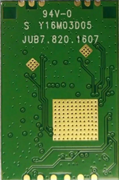
The BL-R8812AF1-A comes in a QFN-32 package with the following pin configuration:

Pin Number Pin Name Description
1 VDD Power supply input (1.8V to 3.6V)
2 GND Ground
3 RF_IN RF input for antenna
4 RF_OUT RF output for antenna
5 TXD Transmit data
6 RXD Receive data
7 SCLK Serial clock for SPI interface
8 MOSI Master Out Slave In (SPI data input)
9 MISO Master In Slave Out (SPI data output)
10 CSN Chip select (active low)
11-32 NC Not connected

Usage Instructions

How to Use the BL-R8812AF1-A in a Circuit

  1. Power Supply: Connect the VDD pin to a stable power source within the range of 1.8V to 3.6V. Ensure proper decoupling capacitors are placed near the VDD pin to reduce noise.
  2. Grounding: Connect the GND pin to the ground plane of the PCB to ensure proper operation and minimize noise.
  3. Antenna Connection: Connect an appropriate 2.4 GHz antenna to the RF_IN and RF_OUT pins. Use impedance-matched traces for optimal performance.
  4. SPI Communication: Use the SCLK, MOSI, MISO, and CSN pins to interface with a microcontroller via the SPI protocol. Ensure the SPI clock speed is compatible with the transceiver's specifications.
  5. Data Transmission and Reception: Use the TXD and RXD pins to send and receive data. Configure the modulation scheme and data rate as required by your application.

Important Considerations and Best Practices

  • PCB Layout: Ensure proper grounding and minimize trace lengths for RF signals to reduce losses and interference.
  • Antenna Matching: Use an impedance-matching network to optimize the antenna's performance.
  • Power Management: Use low-dropout regulators (LDOs) or DC-DC converters to provide a stable power supply.
  • Firmware Configuration: Configure the transceiver's registers via SPI to set the desired frequency, modulation scheme, and data rate.

Example: Connecting to an Arduino UNO

The BL-R8812AF1-A can be connected to an Arduino UNO for wireless communication. Below is an example of Arduino code to initialize the SPI interface and communicate with the transceiver:

#include <SPI.h>

// Define SPI pins for the BL-R8812AF1-A
#define CSN_PIN 10  // Chip Select (active low)
#define SCLK_PIN 13 // Serial Clock
#define MOSI_PIN 11 // Master Out Slave In
#define MISO_PIN 12 // Master In Slave Out

void setup() {
  // Initialize SPI
  SPI.begin();
  pinMode(CSN_PIN, OUTPUT);
  digitalWrite(CSN_PIN, HIGH); // Set CSN high to deselect the transceiver

  Serial.begin(9600); // Initialize serial communication for debugging
  Serial.println("BL-R8812AF1-A Initialization...");
  
  // Example: Write to a register (replace 0x01 and 0xFF with actual values)
  digitalWrite(CSN_PIN, LOW); // Select the transceiver
  SPI.transfer(0x01);         // Send register address
  SPI.transfer(0xFF);         // Send data to write
  digitalWrite(CSN_PIN, HIGH); // Deselect the transceiver

  Serial.println("Initialization complete.");
}

void loop() {
  // Example: Read data from the transceiver
  digitalWrite(CSN_PIN, LOW); // Select the transceiver
  SPI.transfer(0x02);         // Send register address to read
  byte data = SPI.transfer(0x00); // Read data
  digitalWrite(CSN_PIN, HIGH); // Deselect the transceiver

  Serial.print("Received data: ");
  Serial.println(data, HEX);

  delay(1000); // Wait for 1 second
}

Troubleshooting and FAQs

Common Issues and Solutions

  1. No Communication with the Transceiver

    • Cause: Incorrect SPI connections or configuration.
    • Solution: Verify the SPI pin connections and ensure the SPI clock speed is within the transceiver's specifications.
  2. Poor RF Performance

    • Cause: Improper antenna matching or PCB layout issues.
    • Solution: Use an impedance-matching network and follow best practices for RF PCB design.
  3. High Power Consumption

    • Cause: The transceiver is not entering low-power modes.
    • Solution: Configure the transceiver to enter sleep mode when not in use.
  4. Data Loss or Corruption

    • Cause: Interference or incorrect data rate settings.
    • Solution: Reduce the data rate or use error correction techniques.

FAQs

  • Q: Can the BL-R8812AF1-A operate in other frequency bands?
    A: No, it is designed specifically for the 2.4 GHz ISM band.

  • Q: What is the maximum range of the transceiver?
    A: The range depends on the antenna and environment but typically extends up to 100 meters in open space.

  • Q: Does the transceiver support encryption?
    A: No, encryption must be implemented at the application level.

  • Q: Can I use the BL-R8812AF1-A with a 5V microcontroller?
    A: Yes, but you must use level shifters to interface the 5V logic with the transceiver's 3.3V logic levels.