
How to Use DSPIC33FJ256GP710: Examples, Pinouts, and Specs

 Design with DSPIC33FJ256GP710 in Cirkit Designer
Introduction
The DSPIC33FJ256GP710 is a 16-bit Digital Signal Controller (DSC) from Microchip Technology. It combines the performance of a Digital Signal Processor (DSP) with the simplicity of a microcontroller, making it ideal for applications requiring advanced signal processing and control. This device features 256 KB of Flash memory, 30 KB of RAM, and a wide range of integrated peripherals, enabling efficient and reliable operation in complex embedded systems.
Explore Projects Built with DSPIC33FJ256GP710
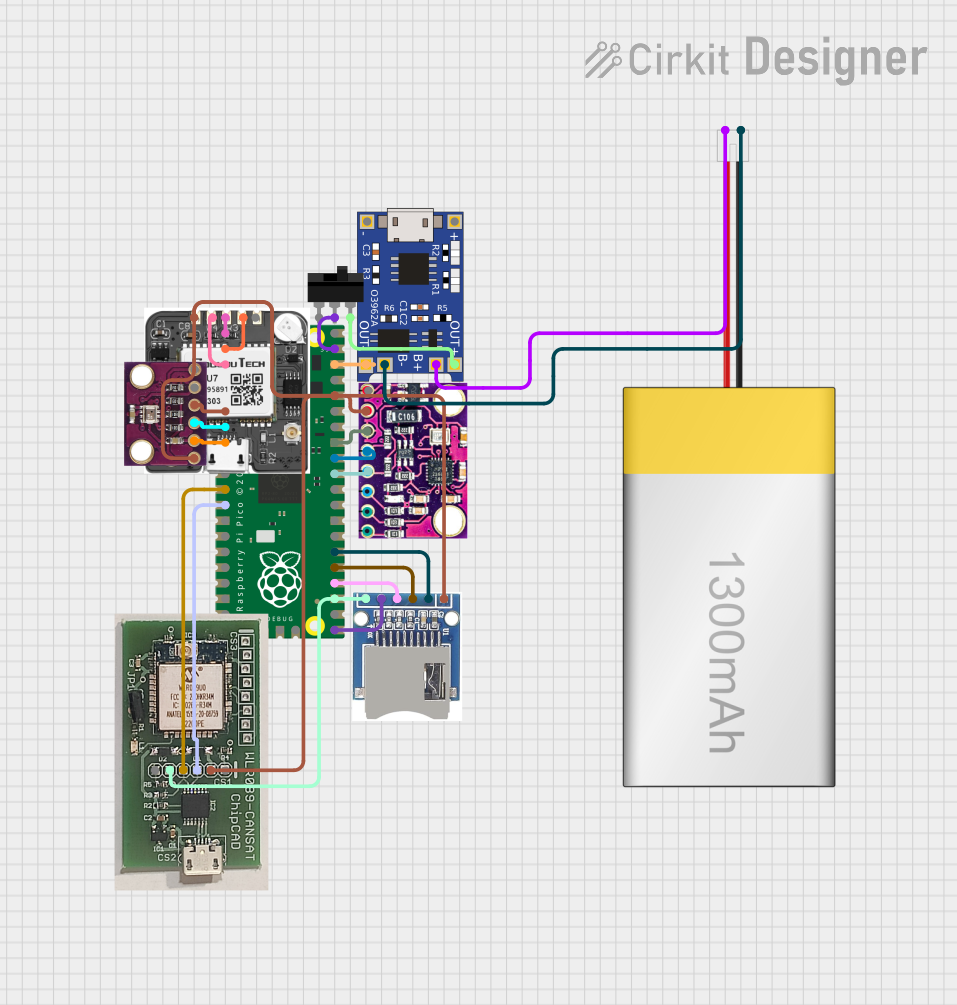 Open Project in Cirkit Designer
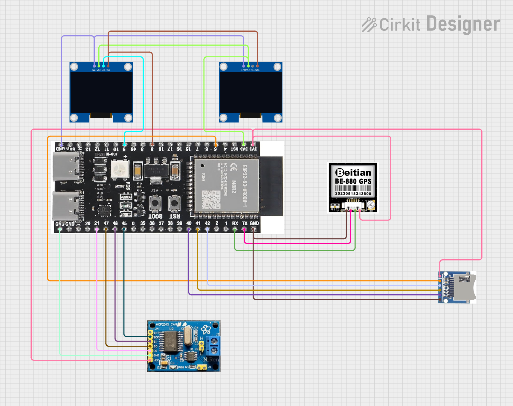 Open Project in Cirkit Designer
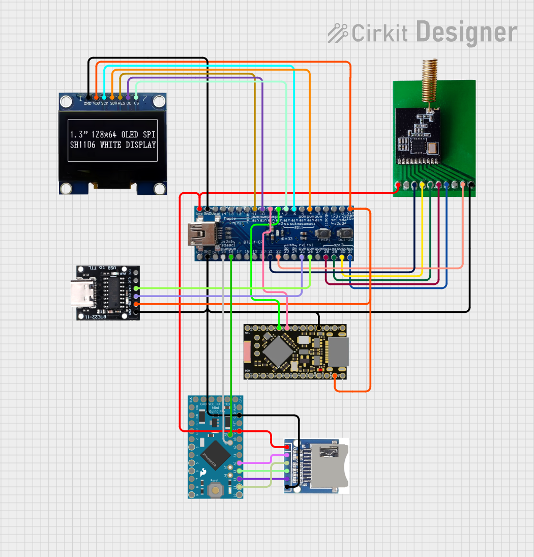 Open Project in Cirkit Designer
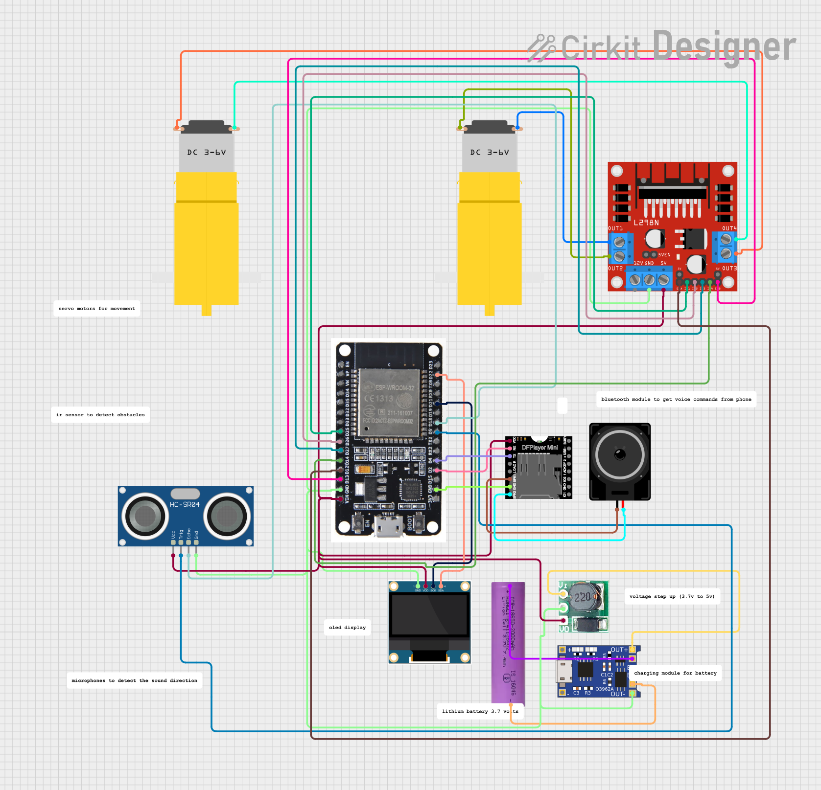 Open Project in Cirkit Designer
Explore Projects Built with DSPIC33FJ256GP710
Open Project in Cirkit DesignerOpen Project in Cirkit DesignerOpen Project in Cirkit DesignerOpen Project in Cirkit DesignerCommon Applications and Use Cases
- Motor control and industrial automation
- Power conversion systems
- Audio and speech processing
- Medical devices
- Embedded control systems
- Advanced communication protocols
Technical Specifications
The following table outlines the key technical specifications of the DSPIC33FJ256GP710:
| Parameter | Value |
|---|---|
| Core Architecture | 16-bit Digital Signal Controller |
| Flash Memory | 256 KB |
| RAM | 30 KB |
| Operating Voltage | 3.0V to 3.6V |
| Clock Speed | Up to 40 MIPS |
| Peripherals | UART, SPI, I2C, CAN, ADC, PWM |
| ADC Resolution | 10-bit or 12-bit (configurable) |
| Timers | 16-bit and 32-bit timers |
| Communication Interfaces | 4 UART, 3 SPI, 2 I2C, 2 CAN |
| GPIO Pins | 85 |
| Package Options | TQFP, QFN |
Pin Configuration and Descriptions
The DSPIC33FJ256GP710 comes in a 100-pin package. Below is a summary of key pin functions:
| Pin Name | Function | Description |
|---|---|---|
| VDD | Power Supply | Connect to 3.3V power supply. |
| VSS | Ground | Connect to ground. |
| OSC1/CLKI | Oscillator Input/Clock Input | External clock or crystal input. |
| OSC2/CLKO | Oscillator Output/Clock Out | External clock or crystal output. |
| ANx | Analog Input | ADC input channels (e.g., AN0, AN1, etc.). |
| PGDx/PGCx | Programming/Debugging Pins | Used for ICSP and debugging (e.g., PGD1, PGC1). |
| RXx/TXx | UART Receive/Transmit | UART communication pins (e.g., RX1, TX1). |
| SCLx/SDAx | I2C Clock/Data | I2C communication pins (e.g., SCL1, SDA1). |
| SCKx/SDIx/SDOx | SPI Clock/Data In/Data Out | SPI communication pins (e.g., SCK1, SDI1, SDO1). |
| PWMx | Pulse Width Modulation | PWM output pins for motor control. |
Refer to the official datasheet for a complete pinout and detailed descriptions.
Usage Instructions
How to Use the DSPIC33FJ256GP710 in a Circuit
- Power Supply: Connect the VDD pin to a 3.3V regulated power supply and the VSS pin to ground.
- Clock Configuration: Use an external crystal oscillator or a clock source connected to the OSC1 and OSC2 pins. Alternatively, configure the internal oscillator.
- Programming and Debugging: Connect the PGD and PGC pins to a compatible programmer/debugger (e.g., Microchip's ICD3 or PICkit).
- Peripheral Configuration: Configure the desired peripherals (e.g., UART, SPI, ADC) in the firmware using Microchip's MPLAB X IDE and XC16 compiler.
- GPIO Usage: Use the GPIO pins for digital input/output operations. Configure them as input or output in the firmware.
Important Considerations and Best Practices
- Voltage Levels: Ensure all input signals are within the 3.3V operating range to avoid damage.
- Decoupling Capacitors: Place decoupling capacitors (e.g., 0.1 µF) close to the VDD pins to reduce noise.
- Clock Stability: Use a stable clock source for reliable operation, especially in time-critical applications.
- Peripheral Initialization: Properly initialize all peripherals in the firmware before use.
- Programming: Use the Integrated Circuit Serial Programming (ICSP) interface for programming the device.
Example Code for UART Communication with Arduino UNO
Below is an example of how to set up UART communication between the DSPIC33FJ256GP710 and an Arduino UNO:
// DSPIC33FJ256GP710 UART Configuration Example
#include <xc.h>

// Configuration bits (adjust as needed for your setup)
#pragma config FOSC = FRC       // Internal Fast RC Oscillator
#pragma config FWDTEN = OFF     // Watchdog Timer Disabled

void UART1_Init(void) {
    U1MODE = 0x0000;            // Clear UART1 mode register
    U1BRG = 25;                 // Baud rate = 9600 (assuming Fcy = 16 MHz)
    U1STA = 0x0400;             // Enable UART1 transmit
    U1MODEbits.UARTEN = 1;      // Enable UART1 module
    U1STAbits.UTXEN = 1;        // Enable UART1 transmitter
}

void UART1_Write(char data) {
    while (U1STAbits.UTXBF);    // Wait until transmit buffer is empty
    U1TXREG = data;             // Transmit data
}

int main(void) {
    UART1_Init();               // Initialize UART1
    while (1) {
        UART1_Write('H');       // Send 'H' over UART
        UART1_Write('i');       // Send 'i' over UART
        UART1_Write('\n');      // Send newline character
        __delay_ms(1000);       // Delay 1 second
    }
    return 0;
}
Notes:
- Connect the DSPIC33FJ256GP710's UART TX pin to the Arduino UNO's RX pin.
- Ensure both devices share a common ground.
Troubleshooting and FAQs
Common Issues
Device Not Responding:
- Cause: Incorrect power supply or clock configuration.
- Solution: Verify the power supply voltage (3.3V) and ensure the clock source is properly configured.
Programming Failure:
- Cause: Incorrect ICSP connections or unsupported programmer.
- Solution: Check the connections to the PGD and PGC pins. Use a compatible programmer (e.g., PICkit or ICD3).
Peripheral Not Working:
- Cause: Peripheral not initialized or misconfigured.
- Solution: Double-check the firmware initialization code for the peripheral.
UART Communication Issues:
- Cause: Baud rate mismatch or incorrect wiring.
- Solution: Ensure the baud rate is the same on both devices and verify the TX/RX connections.
FAQs
Q: Can I use the DSPIC33FJ256GP710 with 5V logic?
- A: No, the DSPIC33FJ256GP710 operates at 3.3V. Use level shifters for interfacing with 5V logic.
Q: What is the maximum clock speed of the DSPIC33FJ256GP710?
- A: The device can operate at up to 40 MIPS with a 40 MHz clock.
Q: How many ADC channels are available?
- A: The DSPIC33FJ256GP710 supports up to 16 ADC channels.
Q: Can I use the internal oscillator instead of an external crystal?
- A: Yes, the internal oscillator can be used, but an external crystal is recommended for higher accuracy.
This concludes the documentation for the DSPIC33FJ256GP710. For more details, refer to the official datasheet and reference manual.