How to Use IC 7483: Examples, Pinouts, and Specs
Introduction
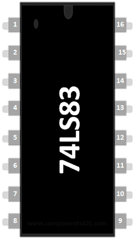
The IC 7483, also known as the 74LS83, is a 4-bit full adder chip that performs the addition of two 4-bit binary numbers. This integrated circuit is essential in digital electronics for executing binary addition, which is a fundamental operation in arithmetic logic units (ALUs) within CPUs, digital counters, and various other computational circuits. The IC 7483 is designed to offer high-speed performance while maintaining low power consumption, making it suitable for a wide range of applications.
Explore Projects Built with IC 7483
Explore Projects Built with IC 7483
Common Applications and Use Cases
- Arithmetic logic units (ALUs) in microprocessors
- Digital counters and timers
- Binary calculators
- Complex digital system computations
Technical Specifications
Key Technical Details
- Supply Voltage (Vcc): 4.75V to 5.25V
- Operating Temperature: 0°C to 70°C
- Logic Family: TTL (Transistor-Transistor Logic)
- Propagation Delay Time: Typically 23 ns
Pin Configuration and Descriptions
| Pin Number | Name | Description |
|---|---|---|
| 1 | A1 | First bit of the first 4-bit input number (LSB) |
| 2 | B1 | First bit of the second 4-bit input number (LSB) |
| 3 | Σ1 | Sum output for the first bit (LSB) |
| 4 | Σ2 | Sum output for the second bit |
| 5 | A2 | Second bit of the first 4-bit input number |
| 6 | B2 | Second bit of the second 4-bit input number |
| 7 | GND | Ground (0V) |
| 8 | A3 | Third bit of the first 4-bit input number |
| 9 | B3 | Third bit of the second 4-bit input number |
| 10 | Σ3 | Sum output for the third bit |
| 11 | Σ4 | Sum output for the fourth bit (MSB) |
| 12 | A4 | Fourth bit of the first 4-bit input number (MSB) |
| 13 | B4 | Fourth bit of the second 4-bit input number (MSB) |
| 14 | Cn+4 | Carry output |
| 15 | Cn | Carry input |
| 16 | Vcc | Positive supply voltage |
Usage Instructions
How to Use the Component in a Circuit
- Connect Vcc (pin 16) to a +5V power supply and GND (pin 7) to the ground.
- Apply the first 4-bit binary number to pins A1 through A4.
- Apply the second 4-bit binary number to pins B1 through B4.
- If there is an incoming carry from a previous stage, connect it to the Cn (pin 15).
- The sum outputs will be available on pins Σ1 through Σ4, and the carry output will be on pin Cn+4.
Important Considerations and Best Practices
- Ensure that the power supply voltage is within the specified range to prevent damage.
- Use decoupling capacitors close to the Vcc and GND pins to stabilize the power supply.
- Avoid floating inputs by connecting unused input pins to either Vcc or GND, as appropriate.
- When cascading multiple 74LS83 chips for more than 4-bit addition, connect the Cn+4 (carry output) of the lower stage to the Cn (carry input) of the next higher stage.
Troubleshooting and FAQs
Common Issues Users Might Face
- Incorrect Outputs: Ensure that all inputs are correctly applied and that there is no floating input.
- No Output: Check the power supply connections and verify that the chip is receiving power.
- Overheating: Make sure the supply voltage is within the recommended range and that the chip is not being overloaded.
Solutions and Tips for Troubleshooting
- Double-check the wiring and connections for any possible errors.
- Use an oscilloscope or logic analyzer to check the signals at the inputs and outputs.
- Replace the IC if it is suspected to be faulty after ruling out other issues.
FAQs
Q: Can the 74LS83 add more than 4-bit numbers? A: Yes, by cascading multiple 74LS83 chips, you can add numbers larger than 4 bits.
Q: What is the maximum speed of the 74LS83? A: The maximum speed is determined by the propagation delay, which is typically 23 ns.
Q: Can the 74LS83 operate with a 3.3V supply? A: No, the 74LS83 is designed for a 5V TTL logic level and may not operate correctly at 3.3V.
Example Connection with Arduino UNO
// Example code for interfacing IC 7483 (74LS83) with Arduino UNO
// This example assumes that the Arduino UNO is used to simulate the inputs to the 74LS83
// and read the outputs. The actual addition logic is performed by the 74LS83.

// Define the Arduino pins connected to the 74LS83
const int inputPins[8] = {2, 3, 4, 5, 6, 7, 8, 9}; // A1, A2, A3, A4, B1, B2, B3, B4
const int outputPins[5] = {10, 11, 12, 13, A0}; // Σ1, Σ2, Σ3, Σ4, Cn+4

void setup() {
  // Initialize all input pins as outputs from the Arduino
  for (int i = 0; i < 8; i++) {
    pinMode(inputPins[i], OUTPUT);
  }

  // Initialize all output pins as inputs to the Arduino
  for (int i = 0; i < 5; i++) {
    pinMode(outputPins[i], INPUT);
  }
}

void loop() {
  // Example: Adding binary numbers 1010 (A) and 1100 (B) with no initial carry
  digitalWrite(inputPins[0], HIGH); // A1
  digitalWrite(inputPins[1], LOW);  // A2
  digitalWrite(inputPins[2], HIGH); // A3
  digitalWrite(inputPins[3], LOW);  // A4

  digitalWrite(inputPins[4], HIGH); // B1
  digitalWrite(inputPins[5], HIGH); // B2
  digitalWrite(inputPins[6], LOW);  // B3
  digitalWrite(inputPins[7], LOW);  // B4

  // Read the sum and carry outputs from the 74LS83
  int sum = 0;
  for (int i = 0; i < 4; i++) {
    sum |= digitalRead(outputPins[i]) << i;
  }
  int carry = digitalRead(outputPins[4]);

  // Print the result in binary form
  Serial.begin(9600);
  Serial.print("Sum: ");
  Serial.println(sum, BIN);
  Serial.print("Carry: ");
  Serial.println(carry, BIN);

  // Wait a bit before the next calculation
  delay(1000);
}
Note: This example code is for demonstration purposes only. In a real-world application, the Arduino would typically be used to control other aspects of the system rather than simulating binary inputs to the 74LS83.