How to Use ADS1292: Examples, Pinouts, and Specs
Introduction
The ADS1292 is a low-power, 24-bit analog-to-digital converter (ADC) designed specifically for biopotential measurements, such as electrocardiogram (ECG) and electroencephalogram (EEG) applications. This highly integrated device includes programmable gain amplifiers (PGAs), a high-speed serial interface, and supports multiple channels for simultaneous data acquisition. Its compact design and low power consumption make it ideal for portable and wearable medical devices.
Explore Projects Built with ADS1292
Explore Projects Built with ADS1292
Common Applications and Use Cases
- Electrocardiogram (ECG) monitoring
- Electroencephalogram (EEG) monitoring
- Portable and wearable medical devices
- Patient monitoring systems
- Research and development in biopotential signal processing
Technical Specifications
Key Technical Details
- Resolution: 24-bit
- Number of Channels: 2 differential input channels
- Input Voltage Range: ±2.4 V (with 2.4 V reference)
- Programmable Gain Amplifier (PGA) Gains: 1, 2, 3, 4, 6, 8, 12
- Data Rate: 125 SPS to 32 kSPS
- Power Supply Voltage: 2.7 V to 5.25 V
- Power Consumption: 335 µW (at 2.4 V, 500 SPS)
- Communication Interface: SPI (Serial Peripheral Interface)
- Operating Temperature Range: -40°C to +85°C
- Package: TQFN-28 (Thin Quad Flat No-lead)
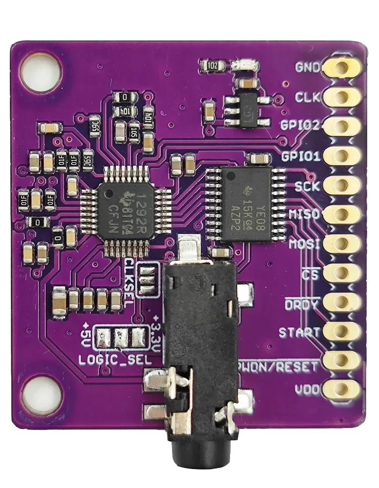
Pin Configuration and Descriptions
The ADS1292 comes in a 28-pin TQFN package. Below is the pin configuration and description:
| Pin Number | Pin Name | Type | Description |
|---|---|---|---|
| 1 | DVDD | Power | Digital power supply (1.8 V to 3.6 V). |
| 2 | DGND | Ground | Digital ground. |
| 3 | START | Digital Input | Start signal to begin conversions. |
| 4 | CS | Digital Input | Chip select for SPI communication. |
| 5 | SCLK | Digital Input | SPI clock input. |
| 6 | DIN | Digital Input | SPI data input. |
| 7 | DOUT | Digital Output | SPI data output. |
| 8 | DRDY | Digital Output | Data ready signal, indicates new data is available. |
| 9 | RESET | Digital Input | Resets the device. |
| 10 | AVDD | Power | Analog power supply (2.7 V to 5.25 V). |
| 11 | AGND | Ground | Analog ground. |
| 12-13 | IN1P, IN1N | Analog Input | Positive and negative inputs for Channel 1. |
| 14-15 | IN2P, IN2N | Analog Input | Positive and negative inputs for Channel 2. |
| 16 | REFOUT | Analog Output | Reference voltage output. |
| 17 | REFIN | Analog Input | Reference voltage input. |
| 18 | CLKSEL | Digital Input | Clock source selection (internal or external). |
| 19 | CLK | Digital Input | External clock input. |
| 20 | GPIO1 | Digital I/O | General-purpose input/output pin 1. |
| 21 | GPIO2 | Digital I/O | General-purpose input/output pin 2. |
| 22-28 | NC | - | No connection. |
Usage Instructions
How to Use the ADS1292 in a Circuit
- Power Supply: Connect the analog (AVDD) and digital (DVDD) power supplies to appropriate voltage levels (e.g., 3.3 V). Ensure proper decoupling capacitors are placed near the power pins.
- Input Signals: Connect the biopotential signals (e.g., ECG electrodes) to the differential input pins (IN1P/IN1N and IN2P/IN2N). Use proper filtering to reduce noise.
- Reference Voltage: Use the internal reference voltage (REFOUT) or provide an external reference voltage to the REFIN pin.
- Clock Source: Select the clock source using the CLKSEL pin. If using an external clock, connect it to the CLK pin.
- SPI Communication: Connect the SPI pins (CS, SCLK, DIN, DOUT) to a microcontroller or processor for data acquisition and configuration.
- Start Conversion: Use the START pin to initiate conversions. Monitor the DRDY pin to check when new data is available.
Important Considerations and Best Practices
- Input Impedance: Ensure the input impedance of the biopotential signals matches the ADS1292's input characteristics to avoid signal distortion.
- Filtering: Use low-pass filters to remove high-frequency noise from the input signals.
- Grounding: Maintain a proper ground plane to minimize noise and interference.
- ESD Protection: Add ESD protection diodes to the input pins to protect the device from electrostatic discharge.
- SPI Configuration: Configure the SPI interface correctly (e.g., clock polarity and phase) to ensure reliable communication.
Example Code for Arduino UNO
Below is an example of how to interface the ADS1292 with an Arduino UNO using SPI:
#include <SPI.h>

// Pin definitions
const int CS_PIN = 10;  // Chip select pin
const int DRDY_PIN = 2; // Data ready pin

void setup() {
  // Initialize SPI
  SPI.begin();
  SPI.setDataMode(SPI_MODE1); // Clock polarity and phase
  SPI.setClockDivider(SPI_CLOCK_DIV16); // Set SPI clock speed
  pinMode(CS_PIN, OUTPUT);
  pinMode(DRDY_PIN, INPUT);
  digitalWrite(CS_PIN, HIGH); // Set CS high (inactive)

  // Reset ADS1292
  resetADS1292();
  configureADS1292();
}

void loop() {
  if (digitalRead(DRDY_PIN) == LOW) { // Check if data is ready
    digitalWrite(CS_PIN, LOW); // Select ADS1292
    uint8_t data = SPI.transfer(0x00); // Read data (example)
    digitalWrite(CS_PIN, HIGH); // Deselect ADS1292
    Serial.println(data); // Print data to serial monitor
  }
}

void resetADS1292() {
  digitalWrite(CS_PIN, LOW);
  SPI.transfer(0x06); // Send RESET command
  digitalWrite(CS_PIN, HIGH);
  delay(100); // Wait for reset to complete
}

void configureADS1292() {
  digitalWrite(CS_PIN, LOW);
  SPI.transfer(0x41); // Write to CONFIG1 register
  SPI.transfer(0x02); // Set data rate to 500 SPS
  digitalWrite(CS_PIN, HIGH);
}
Troubleshooting and FAQs
Common Issues and Solutions
No Data Output:
- Ensure the SPI interface is configured correctly (e.g., clock polarity and phase).
- Verify that the START pin is asserted to begin conversions.
- Check the DRDY pin to confirm data is ready before reading.
High Noise in Output:
- Use proper filtering on the input signals to reduce noise.
- Ensure the input signals are within the specified voltage range.
- Verify that the ground connections are solid and free of interference.
Device Not Responding:
- Check the power supply connections and ensure proper voltage levels.
- Verify the SPI connections and ensure the CS pin is toggled correctly.
- Reset the device using the RESET pin or RESET command.
FAQs
Q: Can the ADS1292 operate with a single-ended input?
A: No, the ADS1292 is designed for differential input signals. Single-ended signals must be converted to differential using external circuitry.
Q: What is the maximum sampling rate of the ADS1292?
A: The maximum sampling rate is 32 kSPS, but lower rates can be configured for power savings.
Q: Can I use the ADS1292 with a 5 V microcontroller?
A: Yes, as long as the digital power supply (DVDD) is compatible with the microcontroller's logic levels. Use level shifters if necessary.