How to Use Quad 2-Input NOR: Examples, Pinouts, and Specs

Introduction
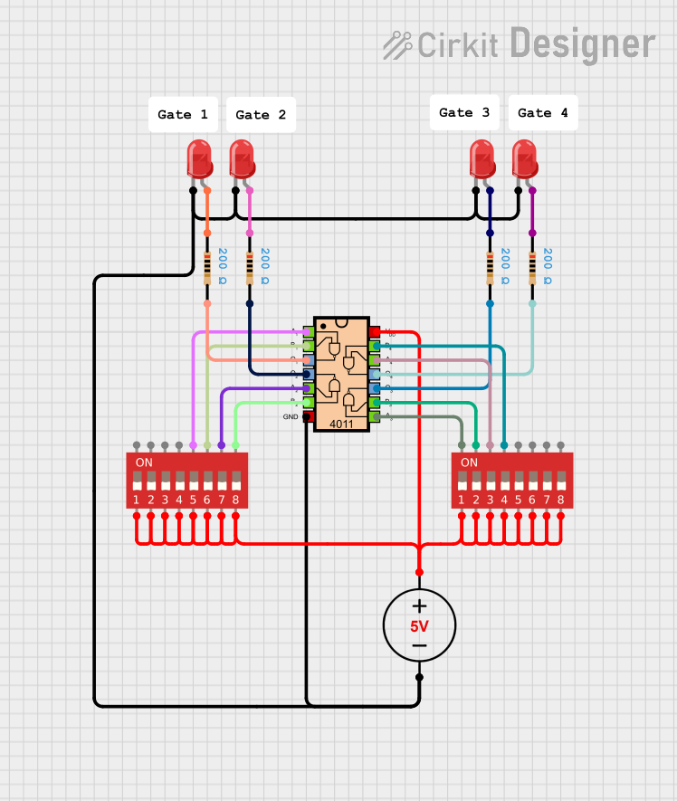
The Quad 2-Input NOR is a digital logic component that contains four independent NOR gates, each with two inputs. A NOR gate is a fundamental building block in digital electronics, performing the logical NOR operation. The output of each gate is low (logic 0) when any of its inputs are high (logic 1). Conversely, the output is high (logic 1) only when all inputs are low (logic 0).
This component is widely used in various logic circuits, including combinational and sequential logic designs. Common applications include signal control, logic inversion, and as part of larger integrated circuits in computing and communication systems.
Explore Projects Built with Quad 2-Input NOR
Explore Projects Built with Quad 2-Input NOR
Technical Specifications
- Logic Family: CMOS/TTL (varies by specific IC model, e.g., 7402 for TTL)
- Supply Voltage (Vcc): Typically 3V to 15V (CMOS) or 4.75V to 5.25V (TTL)
- Input Voltage (VIH/VIL): High-level input voltage (VIH) and low-level input voltage (VIL) depend on the logic family.
- Output Current (IO): Typically ±8mA (TTL) or ±25mA (CMOS)
- Propagation Delay: ~10ns to 50ns (varies by model and supply voltage)
- Power Dissipation: ~10mW to 100mW per gate (varies by logic family)
Pin Configuration and Descriptions
The Quad 2-Input NOR gate is commonly available in a 14-pin Dual In-line Package (DIP). Below is the pinout for a standard 7402 IC:
| Pin Number | Pin Name | Description |
|---|---|---|
| 1 | 1A | Input A for NOR Gate 1 |
| 2 | 1B | Input B for NOR Gate 1 |
| 3 | 1Y | Output of NOR Gate 1 |
| 4 | 2A | Input A for NOR Gate 2 |
| 5 | 2B | Input B for NOR Gate 2 |
| 6 | 2Y | Output of NOR Gate 2 |
| 7 | GND | Ground (0V) |
| 8 | 3Y | Output of NOR Gate 3 |
| 9 | 3A | Input A for NOR Gate 3 |
| 10 | 3B | Input B for NOR Gate 3 |
| 11 | 4Y | Output of NOR Gate 4 |
| 12 | 4A | Input A for NOR Gate 4 |
| 13 | 4B | Input B for NOR Gate 4 |
| 14 | Vcc | Positive Supply Voltage |
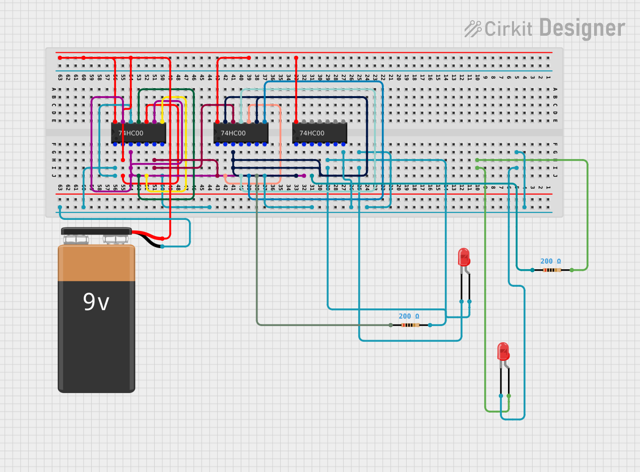
Usage Instructions
How to Use the Component in a Circuit
- Power Supply: Connect the Vcc pin (Pin 14) to the positive supply voltage and the GND pin (Pin 7) to ground.
- Inputs: Provide logic signals to the input pins (e.g., 1A, 1B, etc.). Ensure the input voltage levels are within the specified range for the logic family.
- Outputs: The output pins (e.g., 1Y, 2Y, etc.) will provide the NOR operation result. Connect these outputs to other components or circuits as needed.
Example Circuit
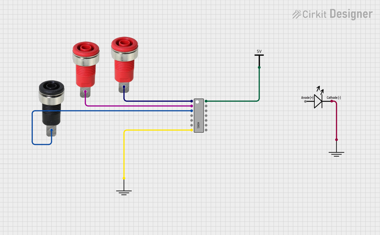
To demonstrate the NOR gate operation, connect the inputs of one gate (e.g., 1A and 1B) to switches or logic sources. Connect the output (1Y) to an LED with a current-limiting resistor. The LED will light up only when both inputs are low.
Arduino UNO Example
The Quad 2-Input NOR can be interfaced with an Arduino UNO to demonstrate its functionality. Below is an example code snippet:
// Example: Using a Quad 2-Input NOR gate with Arduino UNO
// This code demonstrates the NOR operation by reading two digital inputs
// and outputting the result to an LED.

const int inputA = 2;  // Pin 2 connected to 1A of the NOR gate
const int inputB = 3;  // Pin 3 connected to 1B of the NOR gate
const int outputY = 4; // Pin 4 connected to 1Y of the NOR gate

void setup() {
  pinMode(inputA, OUTPUT);  // Set inputA as an output pin
  pinMode(inputB, OUTPUT);  // Set inputB as an output pin
  pinMode(outputY, INPUT);  // Set outputY as an input pin
  Serial.begin(9600);       // Initialize serial communication
}

void loop() {
  digitalWrite(inputA, LOW);  // Set inputA to LOW
  digitalWrite(inputB, LOW);  // Set inputB to LOW
  delay(1000);                // Wait for 1 second

  int norOutput = digitalRead(outputY);  // Read the NOR gate output
  Serial.print("NOR Output: ");
  Serial.println(norOutput);  // Print the output to the Serial Monitor

  // Change input states to test other conditions
  digitalWrite(inputA, HIGH);  // Set inputA to HIGH
  delay(1000);
  digitalWrite(inputB, HIGH);  // Set inputB to HIGH
  delay(1000);
}
Important Considerations and Best Practices
- Ensure the supply voltage (Vcc) matches the logic family specifications.
- Use pull-up or pull-down resistors on unused inputs to prevent floating states.
- Avoid exceeding the maximum current ratings to prevent damage to the IC.
- Decouple the power supply with a capacitor (e.g., 0.1µF) near the IC to reduce noise.
Troubleshooting and FAQs
Common Issues
No Output Signal:
- Check the power supply connections (Vcc and GND).
- Verify that the input signals are within the specified voltage range.
- Ensure the output is not overloaded or short-circuited.
Incorrect Output:
- Confirm the logic levels of the inputs.
- Check for floating inputs and use pull-up or pull-down resistors if necessary.
Overheating:
- Ensure the IC is not drawing excessive current.
- Verify that the supply voltage is within the recommended range.
FAQs
Q: Can I use the Quad 2-Input NOR gate with a 3.3V system?
A: Yes, if you are using a CMOS version of the IC that supports a 3.3V supply. Check the datasheet for compatibility.
Q: What happens if I leave an input pin unconnected?
A: Unconnected inputs can cause unpredictable behavior due to floating states. Always tie unused inputs to Vcc or GND through a resistor.
Q: How do I test the IC to ensure it is functioning correctly?
A: Use a multimeter or logic probe to verify the output for various input combinations. Alternatively, connect the IC to a simple test circuit with LEDs to observe the logic operation.