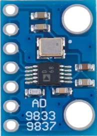
How to Use AD9833/9837: Examples, Pinouts, and Specs
Introduction
The AD9833/9837 is a low-power, programmable waveform generator designed to produce sine, square, and triangular waveforms. It operates using a serial interface, making it highly versatile and easy to integrate into digital systems. This component is widely used in applications such as signal generation, function generation, frequency synthesis, and phase modulation.
The AD9833/9837 is ideal for applications requiring precise waveform generation with minimal power consumption. Its compact design and programmability make it suitable for use in portable devices, communication systems, and test equipment.
Explore Projects Built with AD9833/9837
Explore Projects Built with AD9833/9837
Technical Specifications
Below are the key technical details for the AD9833/9837:
- Supply Voltage (VDD): 2.3 V to 5.5 V
- Power Consumption: ~20 mW at 3 V
- Output Frequency Range: Up to 12.5 MHz
- Waveform Types: Sine, square, and triangular
- Interface: Serial Peripheral Interface (SPI)
- Resolution:
- Frequency: 28-bit
- Phase: 12-bit
- Operating Temperature Range: -40°C to +85°C
- Package Options: TSSOP-10 (AD9833), MSOP-10 (AD9837)
Pin Configuration and Descriptions
The AD9833 and AD9837 share a similar pinout. Below is the pin configuration:
| Pin | Name | Description |
|---|---|---|
| 1 | FSYNC | Active-low chip select for SPI communication. |
| 2 | SCLK | Serial clock input for SPI communication. |
| 3 | SDATA | Serial data input for SPI communication. |
| 4 | VDD | Positive power supply (2.3 V to 5.5 V). |
| 5 | CAP/2.5V | Decoupling capacitor pin for the internal 2.5 V regulator. |
| 6 | DGND | Digital ground. |
| 7 | AGND | Analog ground. |
| 8 | COMP | Compensation pin for the internal DAC. |
| 9 | IOUT | Current output for the generated waveform. |
| 10 | RESET | Active-high reset pin. Resets the internal registers and disables the output. |
Usage Instructions
How to Use the AD9833/9837 in a Circuit
Power Supply:
- Connect the VDD pin to a stable power source (2.3 V to 5.5 V).
- Use decoupling capacitors (e.g., 0.1 µF and 10 µF) between VDD and ground to reduce noise.
SPI Communication:
- Connect the FSYNC, SCLK, and SDATA pins to the corresponding SPI pins of your microcontroller.
- Ensure the SPI clock frequency is compatible with the AD9833/9837.
Output Configuration:
- Connect the IOUT pin to a load or an external circuit to use the generated waveform.
- Use a low-pass filter if a clean sine wave is required.
Programming the Waveform:
- Use SPI commands to configure the frequency, phase, and waveform type.
- Refer to the datasheet for the specific register map and command structure.
Important Considerations and Best Practices
- Reset on Power-Up: Always reset the device after power-up by toggling the RESET pin or sending a software reset command.
- Output Impedance: The IOUT pin has a high output impedance. Use a buffer amplifier if driving a low-impedance load.
- Thermal Management: Ensure adequate ventilation or heat dissipation if operating at high frequencies or in warm environments.
- Decoupling Capacitors: Place decoupling capacitors as close as possible to the VDD and CAP/2.5V pins.
Example: Using AD9833 with Arduino UNO
Below is an example of how to interface the AD9833 with an Arduino UNO to generate a sine wave:
#include <SPI.h>

// Define SPI pins for AD9833
#define FSYNC 10  // Chip select pin for AD9833

// Function to send a 16-bit word to the AD9833
void sendToAD9833(uint16_t data) {
  digitalWrite(FSYNC, LOW);  // Select the AD9833
  SPI.transfer(highByte(data));  // Send the high byte
  SPI.transfer(lowByte(data));   // Send the low byte
  digitalWrite(FSYNC, HIGH);  // Deselect the AD9833
}

void setup() {
  // Initialize SPI
  SPI.begin();
  SPI.setDataMode(SPI_MODE2);  // AD9833 uses SPI Mode 2
  SPI.setClockDivider(SPI_CLOCK_DIV16);  // Set SPI clock speed
  pinMode(FSYNC, OUTPUT);
  digitalWrite(FSYNC, HIGH);

  // Reset the AD9833
  sendToAD9833(0x2100);  // Reset command

  // Set frequency to 1 kHz (example value)
  uint32_t freqWord = (1000UL * 268435456UL) / 25000000UL;  // Freq formula
  sendToAD9833(0x4000 | (freqWord & 0x3FFF));  // Lower 14 bits
  sendToAD9833(0x4000 | ((freqWord >> 14) & 0x3FFF));  // Upper 14 bits

  // Set phase to 0
  sendToAD9833(0xC000);

  // Enable sine wave output
  sendToAD9833(0x2000);
}

void loop() {
  // The waveform is generated continuously; no code is needed here.
}
Troubleshooting and FAQs
Common Issues and Solutions
No Output Signal:
- Ensure the FSYNC, SCLK, and SDATA pins are correctly connected to the microcontroller.
- Verify that the SPI clock mode is set to Mode 2.
- Check the power supply and decoupling capacitors.
Distorted Waveform:
- Use a low-pass filter to clean up the output signal.
- Verify that the load impedance is appropriate for the IOUT pin.
Incorrect Frequency or Phase:
- Double-check the frequency and phase register values.
- Ensure the correct formula is used to calculate the frequency word.
Device Not Responding:
- Confirm that the FSYNC pin is toggled correctly during SPI communication.
- Check for loose or incorrect wiring.
FAQs
Q: Can the AD9833/9837 generate multiple waveforms simultaneously?
A: No, the AD9833/9837 can only generate one waveform at a time. You can switch between waveforms by reprogramming the device.
Q: What is the maximum output frequency?
A: The maximum output frequency is approximately 12.5 MHz, but the output quality may degrade at higher frequencies.
Q: Is the AD9833/9837 compatible with 3.3 V systems?
A: Yes, the AD9833/9837 operates with supply voltages as low as 2.3 V, making it compatible with 3.3 V systems.
Q: Do I need an external clock source?
A: No, the AD9833/9837 has an internal clock, but you can use an external clock if higher precision is required.