How to Use 74HC73: Examples, Pinouts, and Specs

Introduction
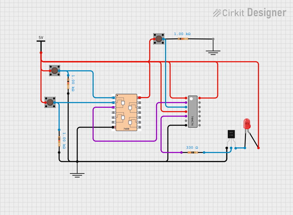
The 74HC73 is a dual JK flip-flop integrated circuit, which is part of the 74HC family of high-speed CMOS devices. It contains two independent flip-flops with JK and negative-edge-triggered inputs. JK flip-flops are versatile and can be used in a variety of digital circuits, including counters, shift registers, and memory storage elements. The 74HC73 is commonly used in applications requiring synchronization and state storage.
Explore Projects Built with 74HC73
Explore Projects Built with 74HC73
Technical Specifications
Key Technical Details
- Supply Voltage (Vcc): 2.0V to 6.0V
- High-Level Input Voltage (VIH): Minimum 2.0V
- Low-Level Input Voltage (VIL): Maximum 0.8V
- Output Current (IO): ±5.2 mA
- Propagation Delay Time: Approximately 13 ns at Vcc = 4.5V, CL = 15 pF
- Operating Temperature Range: -40°C to +125°C
Pin Configuration and Descriptions
| Pin Number | Name | Description |
|---|---|---|
| 1 | 1J | Input to the first flip-flop (J input) |
| 2 | 1\Q | Complementary output from the first flip-flop |
| 3 | 1CLK | Clock input to the first flip-flop (negative-edge triggered) |
| 4 | 1K | Input to the first flip-flop (K input) |
| 5 | 1Q | Output from the first flip-flop |
| 6 | GND | Ground (0V) |
| 7 | 2Q | Output from the second flip-flop |
| 8 | 2K | Input to the second flip-flop (K input) |
| 9 | 2CLK | Clock input to the second flip-flop (negative-edge triggered) |
| 10 | 2\Q | Complementary output from the second flip-flop |
| 11 | 2J | Input to the second flip-flop (J input) |
| 12 | NC | No Connection (should be left floating) |
| 13 | NC | No Connection (should be left floating) |
| 14 | Vcc | Positive supply voltage |
Usage Instructions
How to Use the 74HC73 in a Circuit
Power Supply: Connect the Vcc pin (14) to a positive supply voltage within the range of 2.0V to 6.0V. Connect the GND pin (6) to the ground of the circuit.
Inputs: Apply signals to the J and K inputs of the flip-flops. These inputs determine the state of the flip-flop based on the truth table.
Clocking: Apply a negative-edge-triggered clock pulse to the CLK input. The state of the J and K inputs is read and acted upon on the falling edge of the clock signal.
Outputs: The Q and \Q outputs will reflect the state of the flip-flop after the clock pulse. Q is the normal output, and \Q is the complementary output.
Important Considerations and Best Practices
- Ensure that the supply voltage does not exceed the maximum rating to prevent damage to the IC.
- Unused inputs should be tied to an appropriate logic level (Vcc or GND) to avoid floating inputs, which can lead to unpredictable behavior.
- Decoupling capacitors (typically 0.1 µF) should be placed close to the Vcc pin to filter out noise and provide a stable supply voltage.
- Avoid applying inputs while the chip is not powered, as this can cause current to flow into the inputs and potentially damage the IC.
Troubleshooting and FAQs
Common Issues
- Unstable Outputs: This can be caused by floating inputs or insufficient decoupling. Ensure all inputs are tied to a defined logic level and decoupling capacitors are used.
- No Output Change on Clock Pulse: Verify that the clock pulse is a clean falling edge and that the J and K inputs are set up correctly before the clock edge.
Solutions and Tips for Troubleshooting
- Check the supply voltage and ground connections for proper levels and stability.
- Use an oscilloscope to verify the integrity of the clock signal and the timing of the J and K inputs.
- Ensure that the propagation delay of the flip-flop is accounted for in the timing of your digital circuit.
FAQs
Q: Can the 74HC73 be used as a toggle flip-flop? A: Yes, by connecting the J and K inputs together and applying a high level, the flip-flop will toggle its output on each falling edge of the clock.
Q: What is the purpose of the \Q output? A: The \Q output provides the inverse of the Q output. It can be used in circuits where the complementary state is needed without additional inverting logic.
Q: How can I reset the 74HC73 flip-flops? A: The 74HC73 does not have a direct reset input. To reset the flip-flops, you must control the J and K inputs to set the desired output state on the next clock pulse.
Q: Can I chain multiple 74HC73 ICs together? A: Yes, you can chain multiple ICs to create larger sequential logic circuits. Ensure that the clock signal is distributed cleanly to all flip-flops for proper synchronization.
Example Code for Arduino UNO
The following example demonstrates how to interface the 74HC73 with an Arduino UNO to toggle the state of the flip-flop with a button press.
const int buttonPin = 2; // Button connected to digital pin 2
const int clockPin = 3;  // Clock connected to digital pin 3

void setup() {
  pinMode(buttonPin, INPUT_PULLUP); // Set the button as an input with internal pull-up
  pinMode(clockPin, OUTPUT);        // Set the clock pin as an output
}

void loop() {
  static bool lastButtonState = HIGH; // Store the last state of the button
  bool currentButtonState = digitalRead(buttonPin); // Read the current state of the button

  // Check if button state has changed from HIGH to LOW (button press)
  if (lastButtonState == HIGH && currentButtonState == LOW) {
    // Generate a negative edge on the clock pin
    digitalWrite(clockPin, HIGH);
    delayMicroseconds(5); // Short delay for signal stability
    digitalWrite(clockPin, LOW);
  }

  lastButtonState = currentButtonState; // Update the last button state
}
This code sets up a simple circuit where a button press generates a clock pulse for the 74HC73 flip-flop. The J and K inputs of the flip-flop should be tied to Vcc to configure it as a toggle flip-flop. The Q output will toggle state with each button press.