How to Use TPS61200: Examples, Pinouts, and Specs
Introduction
The TPS61200 is a high-efficiency boost converter integrated circuit (IC) designed to step up a lower input voltage to a higher output voltage. This component is particularly useful in battery-powered applications where maintaining a consistent output voltage is critical as the battery voltage drops over time. Common applications include powering sensors, microcontrollers, and other electronic devices that require a stable voltage supply in portable electronics, energy harvesting, and low-power wireless systems.
Explore Projects Built with TPS61200
Explore Projects Built with TPS61200
Technical Specifications
Key Technical Details
- Input Voltage Range: 0.3 V to 5.5 V
- Output Voltage Range: 1.8 V to 5.5 V (adjustable)
- Maximum Output Current: Up to 1.2 A (depending on input voltage and output voltage)
- Switching Frequency: 1.2 MHz (typical)
- Efficiency: Up to 95% (dependent on input and output conditions)
- Quiescent Current: 55 µA (typical)
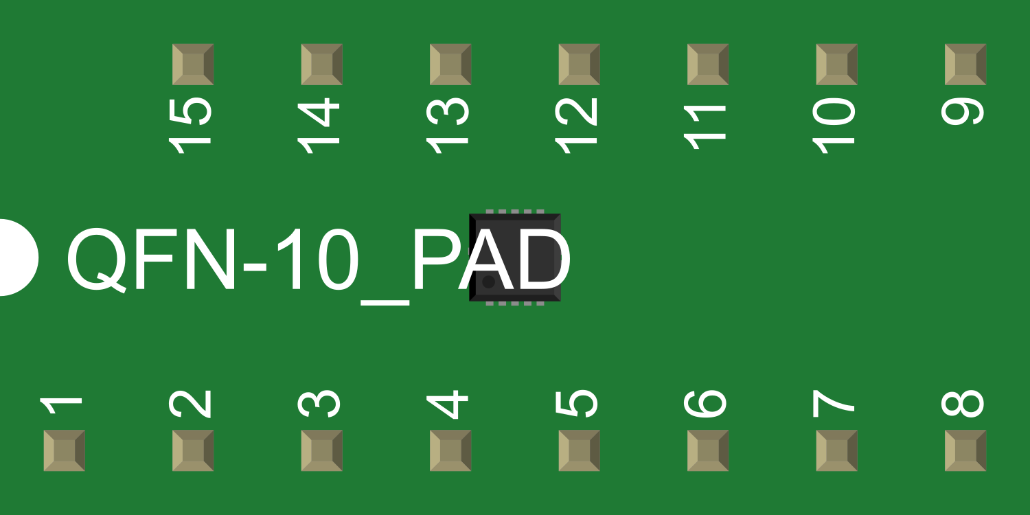
Pin Configuration and Descriptions
| Pin Number | Name | Description |
|---|---|---|
| 1 | GND | Ground reference for the IC. Must be connected to the system ground plane. |
| 2 | L | Connection point for the inductor. |
| 3 | SW | Switch node. Connects to the inductor and Schottky diode. |
| 4 | FB | Feedback pin. Sets the output voltage with an external resistor divider. |
| 5 | VOUT | Output voltage. Connect to the load and the output capacitor. |
| 6 | EN | Enable pin. A logic high enables the IC, while a logic low disables it. |
| 7 | VIN | Input voltage. Connect to the power source and input capacitor. |
| 8 | PG | Power good output. Open-drain output that goes high when VOUT is within regulation. |
Usage Instructions
How to Use the TPS61200 in a Circuit
Input Capacitor: Connect a capacitor (typically 10 µF or greater) between the VIN and GND pins to stabilize the input voltage and provide a low-impedance source for the IC.
Output Capacitor: Connect a capacitor (typically 10 µF or greater) between the VOUT and GND pins to smooth the output voltage and reduce voltage ripple.
Inductor: Choose an inductor with a current rating above the maximum output current of the application. Connect one end to the L pin and the other to the SW pin.
Feedback Network: Connect a resistor divider from VOUT to FB to GND to set the desired output voltage. The values of these resistors can be calculated based on the datasheet formula.
Enable Pin: Connect the EN pin to a logic high level to turn on the IC. If the enable function is not required, this pin can be tied directly to VIN.
Power Good Indicator: The PG pin can be used to monitor the output voltage. Connect a pull-up resistor to a supply voltage if this function is needed.
Important Considerations and Best Practices
- Ensure that the input voltage does not exceed the maximum rating of the IC.
- The layout of the PCB should minimize the loop area formed by the input capacitor, IC, inductor, and output capacitor to reduce electromagnetic interference.
- The feedback network should be placed close to the FB pin and away from noisy components.
- Thermal management should be considered, especially in applications with high output current.
Troubleshooting and FAQs
Common Issues
- Output Voltage Not Regulated: Check the feedback network for correct resistor values and connections. Ensure that the inductor and capacitors meet the specifications.
- IC Overheating: This may be due to excessive output current or inadequate thermal management. Review the current requirements and improve heat dissipation.
- Device Not Powering On: Verify that the EN pin is receiving a logic high signal and that the input voltage is within the specified range.
Solutions and Tips
- If the output voltage is too low, check for short circuits or heavy loads that may be pulling the voltage down.
- For noise-sensitive applications, consider using a lower switching frequency variant or adding filtering components.
- If the device is not enabling properly, ensure that the EN pin voltage exceeds the enable threshold specified in the datasheet.
FAQs
Q: Can the TPS61200 be used to charge batteries? A: The TPS61200 is not a battery charger IC; it is a boost converter designed to provide a stable output voltage.
Q: What is the maximum input voltage the TPS61200 can handle? A: The maximum input voltage is 5.5 V. Exceeding this voltage can damage the IC.
Q: How do I select the correct inductor value? A: The inductor value is chosen based on the desired output current, switching frequency, and efficiency. Refer to the datasheet for guidance on inductor selection.
Q: Is external compensation required for the TPS61200? A: No, the TPS61200 has internal compensation, simplifying the design and reducing external component count.
Example Code for Arduino UNO
Below is an example code snippet for enabling the TPS61200 using an Arduino UNO. This assumes the EN pin of the TPS61200 is connected to a digital I/O pin of the Arduino (e.g., pin 7).
// Define the TPS61200 enable pin
const int enablePin = 7;

void setup() {
  // Set the enable pin as an output
  pinMode(enablePin, OUTPUT);

  // Enable the TPS61200
  digitalWrite(enablePin, HIGH);
}

void loop() {
  // The TPS61200 is now enabled and providing power to the load.
  // Implement application-specific code here.
}
Remember to ensure that the logic level from the Arduino is compatible with the EN pin voltage requirements of the TPS61200.