How to Use 7432 OR Gate IC: Examples, Pinouts, and Specs
Introduction
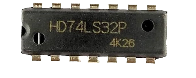
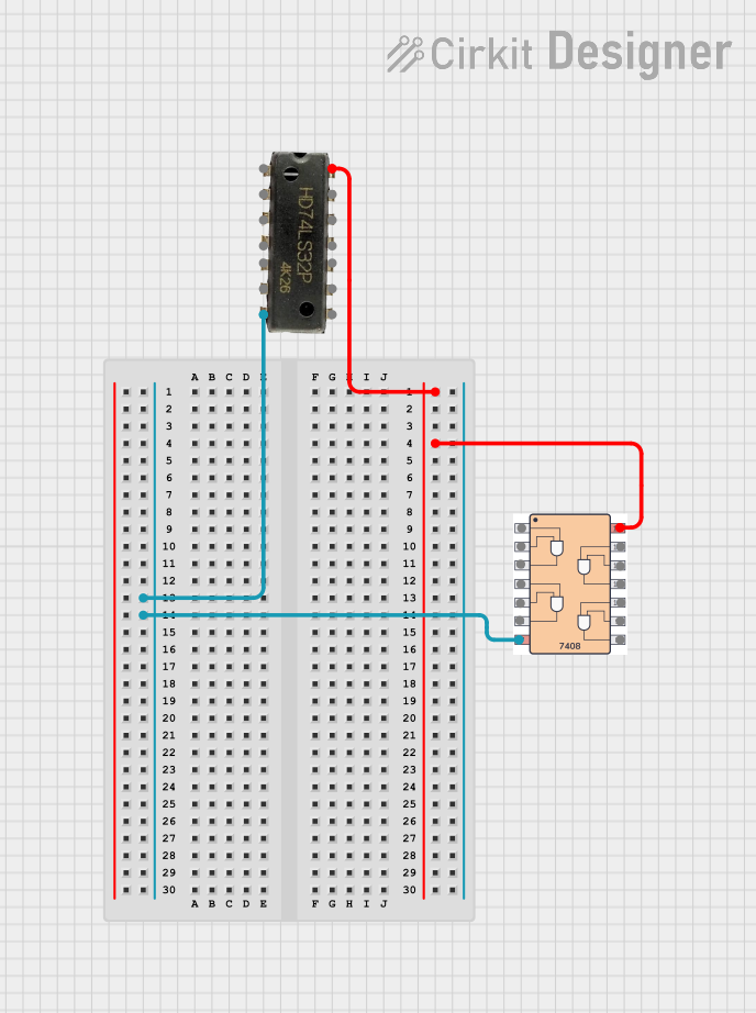
The 7432 Quad 2-Input OR Gate IC is a digital logic integrated circuit that contains four independent OR gates. Each gate has two inputs, labeled A and B, and one output, labeled Y. The OR gate is a fundamental building block in digital electronics, used to create more complex logic circuits. It performs the inclusive OR operation, which means the output is true (high) if at least one of the inputs is true.
Explore Projects Built with 7432 OR Gate IC
Explore Projects Built with 7432 OR Gate IC
Common Applications and Use Cases:
- Digital logic circuits
- Control systems
- Signal processing
- Function generators
- Alarm systems
Technical Specifications
Key Technical Details:
- Supply Voltage (Vcc): 4.75V to 5.25V (Typical TTL levels)
- Input Voltage (Vin): 0V to Vcc
- Output Voltage (Vout): 0V to Vcc (when high)
- High-Level Input Voltage (VIH): Minimum 2V
- Low-Level Input Voltage (VIL): Maximum 0.8V
- High-Level Output Current (IOH): -0.4 mA (Max)
- Low-Level Output Current (IOL): 8 mA (Max)
- Propagation Delay Time: Typically 15 ns
Pin Configuration and Descriptions:
| Pin Number | Description |
|---|---|
| 1 | Input A1 |
| 2 | Input B1 |
| 3 | Output Y1 |
| 4 | Input A2 |
| 5 | Input B2 |
| 6 | Output Y2 |
| 7 | Ground (GND) |
| 8 | Output Y3 |
| 9 | Input B3 |
| 10 | Input A3 |
| 11 | Output Y4 |
| 12 | Input B4 |
| 13 | Input A4 |
| 14 | Supply Voltage (Vcc) |
Usage Instructions
How to Use the Component in a Circuit:
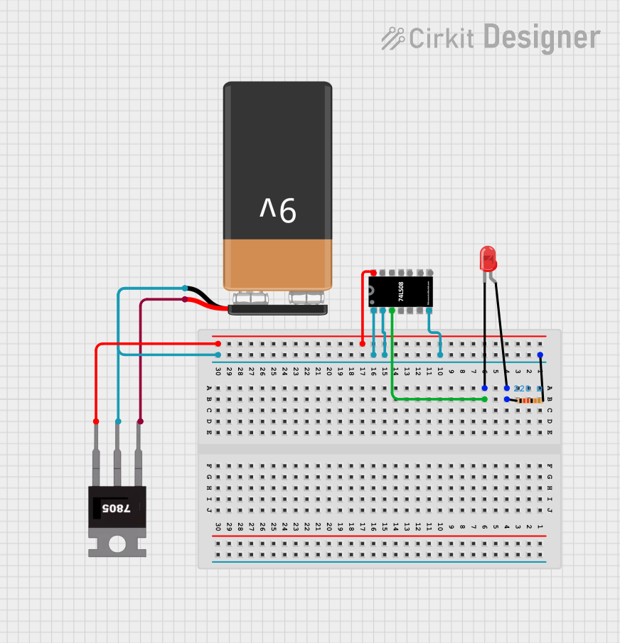
- Connect the Vcc pin (14) to the positive supply voltage (typically +5V).
- Connect the GND pin (7) to the ground of the circuit.
- Apply input signals to the A and B inputs of the OR gates you intend to use.
- The corresponding Y output will be high if at least one of the inputs to the gate is high.
Important Considerations and Best Practices:
- Ensure that the supply voltage does not exceed the maximum rating to prevent damage.
- Unused inputs should be tied to the ground to avoid floating inputs which can lead to unpredictable behavior.
- Decoupling capacitors (typically 0.1 µF) should be placed close to the Vcc pin to filter out noise.
- Avoid loading the output beyond the specified current limits to maintain proper voltage levels.
Troubleshooting and FAQs
Common Issues Users Might Face:
- Output not as expected: Verify that the supply voltage is within the specified range and that all inputs are connected correctly.
- Floating inputs: Ensure that all unused inputs are tied to ground.
- Noise issues: Check for proper decoupling and that the IC is not placed near high-frequency signals if not necessary.
Solutions and Tips for Troubleshooting:
- Double-check wiring and solder joints for any shorts or opens.
- Measure the supply voltage and input signals with a multimeter or oscilloscope to ensure they are within the specified range.
- Replace the IC if it is suspected to be faulty after ruling out other issues.
FAQs:
Q: Can I use the 7432 IC with a 3.3V system? A: The 7432 is designed for TTL levels, and its minimum high-level input voltage is 2V. It may not reliably recognize 3.3V as a high signal.
Q: What happens if I connect more than one input to a high signal? A: The OR gate will output a high signal if one or more inputs are high. Additional high inputs do not affect the output state.
Q: Is there a limit to the frequency of the input signal? A: The maximum frequency of the input signal is limited by the propagation delay of the IC. Ensure that the input signal frequency allows for the output to settle within the required time frame.
Example Code for Arduino UNO
The following example demonstrates how to use the 7432 OR Gate IC with an Arduino UNO to perform a simple OR operation with two inputs and one output.
// Define the input and output pins
const int inputPinA = 2; // Connect to Input A1 of 7432
const int inputPinB = 3; // Connect to Input B1 of 7432
const int outputPin = 13; // Connect to Output Y1 of 7432

void setup() {
  pinMode(inputPinA, INPUT);
  pinMode(inputPinB, INPUT);
  pinMode(outputPin, OUTPUT);
}

void loop() {
  // Read the state of the inputs
  int stateA = digitalRead(inputPinA);
  int stateB = digitalRead(inputPinB);

  // Perform the OR operation and set the output
  digitalWrite(outputPin, stateA || stateB);

  // Delay for debounce
  delay(50);
}
Remember to connect the Arduino's GND to the 7432's GND, and the 5V pin to the Vcc pin of the 7432. The output can be observed with an LED or by reading the state on the Arduino's digital pin 13 with a multimeter or an oscilloscope.