
How to Use ADL400: Examples, Pinouts, and Specs
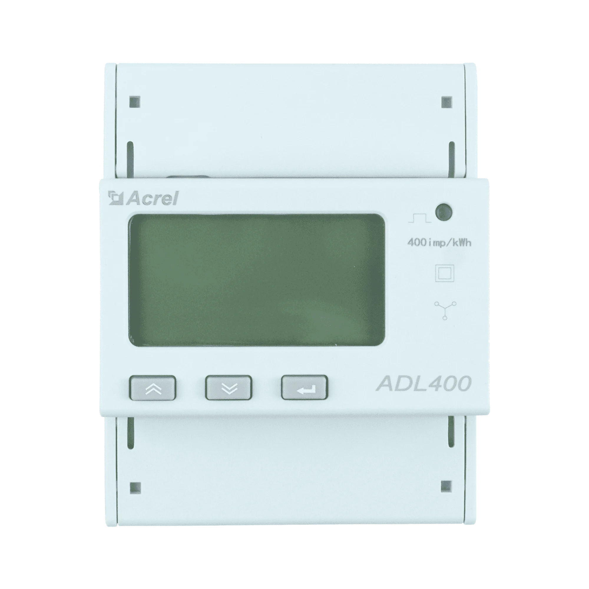
 Design with ADL400 in Cirkit Designer
Introduction
The ADL400 is a high-speed, low-noise analog-to-digital converter (ADC) designed for precision measurement applications. It is engineered to deliver exceptional performance with a wide input voltage range and high resolution, making it ideal for applications requiring accurate signal processing. The ADL400 is commonly used in fields such as instrumentation, medical devices, communication systems, and industrial automation.
Explore Projects Built with ADL400
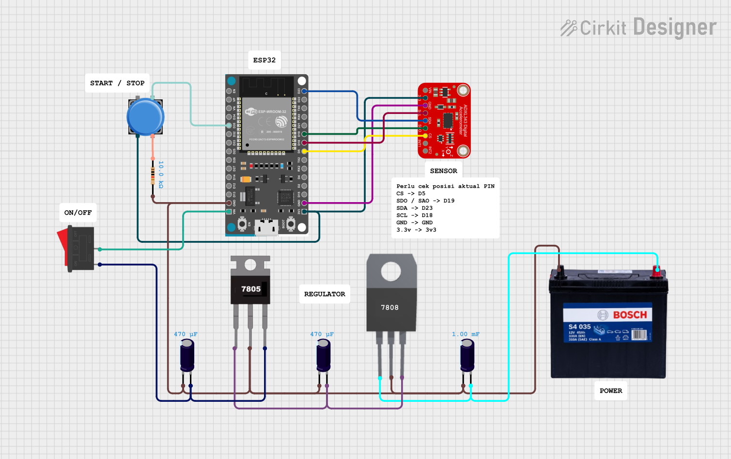 Open Project in Cirkit Designer
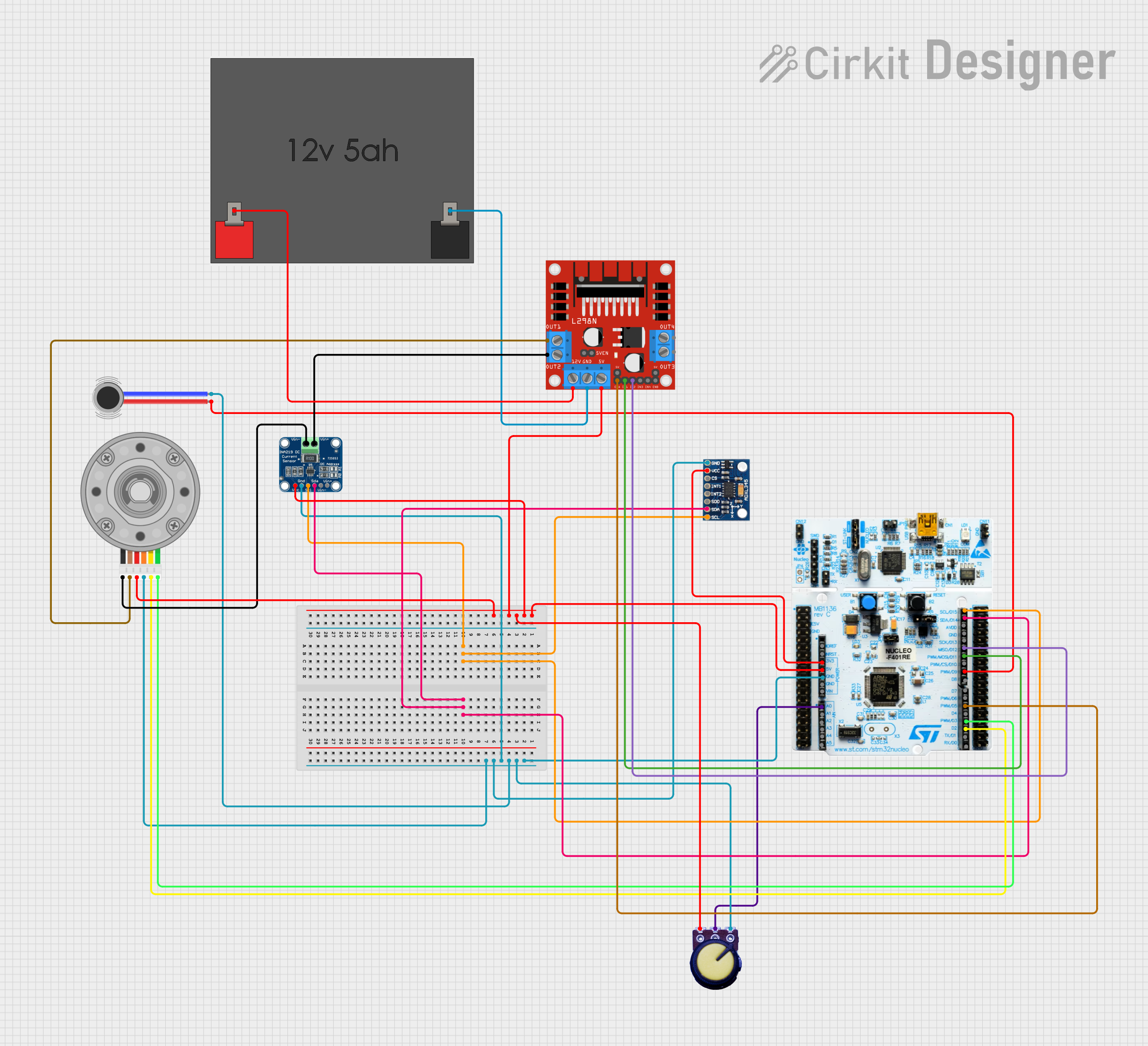 Open Project in Cirkit Designer
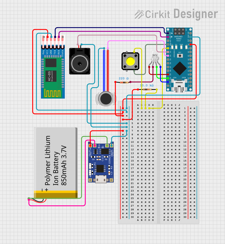 Open Project in Cirkit Designer
 Open Project in Cirkit Designer
Explore Projects Built with ADL400
Open Project in Cirkit DesignerOpen Project in Cirkit DesignerOpen Project in Cirkit DesignerOpen Project in Cirkit DesignerCommon Applications:
- Precision instrumentation and measurement systems
- Medical imaging and diagnostic equipment
- Communication systems requiring high-speed data conversion
- Industrial automation and control systems
- Audio and video signal processing
Technical Specifications
The ADL400 is designed to meet the demands of high-performance applications. Below are its key technical specifications:
| Parameter | Value |
|---|---|
| Resolution | 16-bit |
| Maximum Sampling Rate | 100 MSPS (Mega Samples Per Second) |
| Input Voltage Range | ±5 V |
| Signal-to-Noise Ratio (SNR) | 92 dB |
| Total Harmonic Distortion | -85 dB |
| Power Supply Voltage | 3.3 V or 5 V |
| Power Consumption | 250 mW |
| Operating Temperature Range | -40°C to +85°C |
| Package Type | QFN-32 |
Pin Configuration and Descriptions
The ADL400 comes in a 32-pin QFN (Quad Flat No-lead) package. Below is the pin configuration and description:
| Pin Number | Pin Name | Description |
|---|---|---|
| 1 | VDD | Positive power supply (3.3 V or 5 V) |
| 2 | GND | Ground |
| 3 | VIN+ | Positive analog input |
| 4 | VIN- | Negative analog input |
| 5 | REF+ | Positive reference voltage input |
| 6 | REF- | Negative reference voltage input |
| 7-14 | D0-D7 | Digital output data bits (LSB to MSB) |
| 15 | CLK | Clock input for sampling |
| 16 | OE | Output enable (active low) |
| 17-24 | D8-D15 | Digital output data bits (MSB to LSB) |
| 25 | RESET | Reset input (active low) |
| 26 | CS | Chip select (active low) |
| 27 | RD | Read enable (active low) |
| 28 | WR | Write enable (active low) |
| 29 | TEST | Test mode enable (leave unconnected for normal use) |
| 30 | NC | No connection |
| 31 | VDD | Positive power supply (3.3 V or 5 V) |
| 32 | GND | Ground |
Usage Instructions
How to Use the ADL400 in a Circuit
- Power Supply: Connect the VDD pins to a stable 3.3 V or 5 V power source and the GND pins to ground. Ensure proper decoupling capacitors are placed near the power pins to minimize noise.
- Analog Input: Connect the signal to be converted to the VIN+ and VIN- pins. Use proper filtering to remove unwanted noise from the input signal.
- Reference Voltage: Provide a stable reference voltage to the REF+ and REF- pins. This determines the ADC's input range and accuracy.
- Clock Signal: Supply a clean clock signal to the CLK pin. The sampling rate is determined by the frequency of this clock.
- Digital Outputs: Connect the digital output pins (D0-D15) to a microcontroller, FPGA, or other digital processing unit. Ensure the output enable (OE) pin is properly configured.
- Control Signals: Use the CS, RD, and WR pins to control the ADC's operation. Refer to the timing diagram in the datasheet for proper sequencing.
Important Considerations and Best Practices
- Input Impedance: Ensure the input impedance of the circuit matches the ADC's requirements to avoid signal distortion.
- Decoupling: Use decoupling capacitors (e.g., 0.1 µF and 10 µF) close to the power supply pins to reduce noise.
- Grounding: Implement a proper grounding scheme to minimize ground loops and noise interference.
- Clock Signal Integrity: Use a low-jitter clock source to maintain high conversion accuracy.
- Thermal Management: Ensure adequate cooling if the ADC operates near its maximum power consumption.
Example: Connecting the ADL400 to an Arduino UNO
Below is an example of how to interface the ADL400 with an Arduino UNO for basic data acquisition:
// Example code to read data from the ADL400 ADC using Arduino UNO

#define CLK_PIN 3    // Pin connected to the ADL400 CLK
#define OE_PIN 4     // Pin connected to the ADL400 Output Enable (active low)
#define CS_PIN 5     // Pin connected to the ADL400 Chip Select (active low)
#define DATA_PINS {6, 7, 8, 9, 10, 11, 12, 13} // Arduino digital pins for D0-D7

void setup() {
  // Configure control pins as outputs
  pinMode(CLK_PIN, OUTPUT);
  pinMode(OE_PIN, OUTPUT);
  pinMode(CS_PIN, OUTPUT);

  // Configure data pins as inputs
  for (int i = 0; i < 8; i++) {
    pinMode(DATA_PINS[i], INPUT);
  }

  // Initialize control pins
  digitalWrite(CLK_PIN, LOW);
  digitalWrite(OE_PIN, HIGH); // Disable output initially
  digitalWrite(CS_PIN, HIGH); // Deselect the ADC
}

void loop() {
  // Enable ADC output
  digitalWrite(OE_PIN, LOW);
  digitalWrite(CS_PIN, LOW);

  // Generate a clock pulse
  digitalWrite(CLK_PIN, HIGH);
  delayMicroseconds(1); // Adjust delay based on clock frequency
  digitalWrite(CLK_PIN, LOW);

  // Read data from ADC
  int adcValue = 0;
  for (int i = 0; i < 8; i++) {
    adcValue |= (digitalRead(DATA_PINS[i]) << i);
  }

  // Process or display the ADC value
  Serial.println(adcValue);

  // Disable ADC output
  digitalWrite(CS_PIN, HIGH);
  digitalWrite(OE_PIN, HIGH);

  delay(100); // Adjust sampling interval as needed
}
Troubleshooting and FAQs
Common Issues and Solutions
No Output Data:
- Ensure the OE pin is set to LOW to enable the digital outputs.
- Verify that the CS pin is LOW during data read operations.
Incorrect ADC Values:
- Check the reference voltage (REF+ and REF-) for stability and accuracy.
- Ensure the input signal is within the specified voltage range (±5 V).
High Noise in Output:
- Use proper filtering on the input signal.
- Ensure decoupling capacitors are placed near the power supply pins.
Clock Signal Issues:
- Verify the clock signal frequency matches the desired sampling rate.
- Use a low-jitter clock source for better performance.
FAQs
Q: Can the ADL400 operate at lower sampling rates?
A: Yes, the sampling rate can be adjusted by changing the clock frequency, as long as it remains within the ADC's specified range.
Q: What happens if the input voltage exceeds the specified range?
A: Input voltages beyond the specified range (±5 V) may cause inaccurate conversions or damage the ADC.
Q: Is the ADL400 compatible with 3.3 V logic levels?
A: Yes, the ADL400 supports both 3.3 V and 5 V power supplies, making it compatible with 3.3 V logic systems.
Q: Can I use the ADL400 for audio signal processing?
A: Yes, the ADL400's high resolution and low noise make it suitable for audio applications.