How to Use IC 7476: Examples, Pinouts, and Specs
Introduction
The IC 7476 is a dual D-type flip-flop integrated circuit designed for synchronous data storage and manipulation in digital circuits. It contains two independent flip-flops, each capable of storing one bit of data. Each flip-flop features a data input (D), clock input (CLK), and complementary outputs (Q and Q̅). The IC 7476 is widely used in applications requiring temporary data storage, edge-triggered operations, and sequential logic design.
Explore Projects Built with IC 7476
Explore Projects Built with IC 7476
Common Applications
- Data storage in digital systems
- Shift registers and counters
- Edge-triggered operations
- Sequential logic circuits
- Frequency division and timing circuits
Technical Specifications
The IC 7476 is part of the 74xx series of TTL (Transistor-Transistor Logic) integrated circuits. Below are its key technical specifications:
| Parameter | Value |
|---|---|
| Supply Voltage (Vcc) | 4.75V to 5.25V |
| Input Voltage (VI) | 0V to 5.5V |
| High-Level Input Voltage | Minimum 2V |
| Low-Level Input Voltage | Maximum 0.8V |
| High-Level Output Voltage | Minimum 2.4V (at IOH = -0.4mA) |
| Low-Level Output Voltage | Maximum 0.4V (at IOL = 16mA) |
| Propagation Delay | ~22ns (typical, depending on load) |
| Power Dissipation | ~20mW (typical) |
| Operating Temperature | 0°C to 70°C |
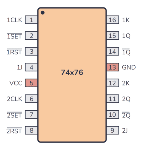
Pin Configuration and Descriptions
The IC 7476 comes in a 14-pin Dual In-line Package (DIP). Below is the pinout and description:
| Pin Number | Pin Name | Description |
|---|---|---|
| 1 | CLR1̅ | Asynchronous Clear for Flip-Flop 1 (Active Low) |
| 2 | CLK1 | Clock Input for Flip-Flop 1 |
| 3 | D1 | Data Input for Flip-Flop 1 |
| 4 | Q1 | Output of Flip-Flop 1 |
| 5 | Q̅1 | Complementary Output of Flip-Flop 1 |
| 6 | PRE1̅ | Asynchronous Preset for Flip-Flop 1 (Active Low) |
| 7 | GND | Ground |
| 8 | PRE2̅ | Asynchronous Preset for Flip-Flop 2 (Active Low) |
| 9 | Q̅2 | Complementary Output of Flip-Flop 2 |
| 10 | Q2 | Output of Flip-Flop 2 |
| 11 | D2 | Data Input for Flip-Flop 2 |
| 12 | CLK2 | Clock Input for Flip-Flop 2 |
| 13 | CLR2̅ | Asynchronous Clear for Flip-Flop 2 (Active Low) |
| 14 | Vcc | Positive Supply Voltage |
Usage Instructions
How to Use the IC 7476 in a Circuit
- Power Supply: Connect pin 14 (Vcc) to a +5V power supply and pin 7 (GND) to ground.
- Data Input: Provide the data to be stored at the D1 (pin 3) and/or D2 (pin 11) inputs.
- Clock Signal: Apply a clock signal to CLK1 (pin 2) and/or CLK2 (pin 12). The flip-flop will store the data present at the D input on the rising edge of the clock signal.
- Outputs: The stored data will appear at Q1 (pin 4) and/or Q2 (pin 10), with the complementary value at Q̅1 (pin 5) and/or Q̅2 (pin 9).
- Asynchronous Control: Use the CLR̅ and PRE̅ pins for asynchronous clear and preset operations:
- Pull CLR̅ low to reset the output (Q = 0, Q̅ = 1).
- Pull PRE̅ low to set the output (Q = 1, Q̅ = 0).
Important Considerations
- Ensure the supply voltage (Vcc) is within the specified range (4.75V to 5.25V).
- Avoid floating inputs; connect unused inputs to a defined logic level (e.g., GND or Vcc).
- Use decoupling capacitors (e.g., 0.1µF) near the IC to reduce noise and stabilize the power supply.
- The IC operates on edge-triggered clock signals; ensure the clock signal has clean rising and falling edges.
Example: Connecting IC 7476 to an Arduino UNO
The IC 7476 can be interfaced with an Arduino UNO to demonstrate its functionality. Below is an example code to toggle the state of a flip-flop using a clock signal generated by the Arduino.
// Example: Toggling IC 7476 Flip-Flop with Arduino UNO
// Pin 2 of Arduino is connected to CLK1 (Pin 2 of IC 7476)
// Pin 3 of Arduino is connected to D1 (Pin 3 of IC 7476)

const int clockPin = 2; // Arduino pin connected to CLK1
const int dataPin = 3;  // Arduino pin connected to D1

void setup() {
  pinMode(clockPin, OUTPUT); // Set clock pin as output
  pinMode(dataPin, OUTPUT);  // Set data pin as output
}

void loop() {
  digitalWrite(dataPin, HIGH); // Set data input to HIGH
  digitalWrite(clockPin, HIGH); // Generate rising edge on clock
  delay(10); // Short delay
  digitalWrite(clockPin, LOW);  // Generate falling edge on clock
  delay(1000); // Wait for 1 second

  digitalWrite(dataPin, LOW);  // Set data input to LOW
  digitalWrite(clockPin, HIGH); // Generate rising edge on clock
  delay(10); // Short delay
  digitalWrite(clockPin, LOW);  // Generate falling edge on clock
  delay(1000); // Wait for 1 second
}
Troubleshooting and FAQs
Common Issues and Solutions
No Output at Q or Q̅:
- Ensure the power supply is connected correctly (Vcc to pin 14, GND to pin 7).
- Verify that the clock signal is being applied to the CLK pin.
- Check that the CLR̅ and PRE̅ pins are not being held low unintentionally.
Unexpected Output States:
- Ensure the D input is stable before the rising edge of the clock signal.
- Avoid noise on the clock line by using proper signal conditioning.
Flip-Flop Not Responding to Clock Signal:
- Verify the clock signal has clean rising and falling edges.
- Check for proper connections and continuity in the circuit.
FAQs
Q1: Can I use the IC 7476 with a 3.3V power supply?
A1: No, the IC 7476 is designed for a 5V TTL logic level. Using a 3.3V supply may result in unreliable operation.
Q2: What happens if both CLR̅ and PRE̅ are pulled low simultaneously?
A2: This condition is not recommended as it may lead to undefined behavior. Ensure only one of these pins is active at a time.
Q3: Can I cascade multiple IC 7476 chips?
A3: Yes, you can cascade multiple IC 7476 chips for applications like shift registers or counters. Ensure proper synchronization of clock signals.