
How to Use 74HC595 SMD: Examples, Pinouts, and Specs
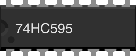
 Design with 74HC595 SMD in Cirkit Designer
Introduction
The 74HC595D by Nexperia is an 8-bit serial-in, parallel-out shift register with an output latch. It is designed for applications requiring efficient pin expansion, such as driving LEDs, 7-segment displays, or other digital outputs. The SMD (Surface Mount Device) version is ideal for compact PCB designs, offering a smaller footprint compared to through-hole components.
Explore Projects Built with 74HC595 SMD
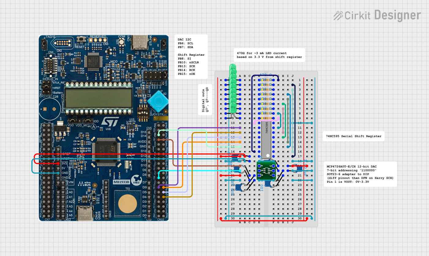 Open Project in Cirkit Designer
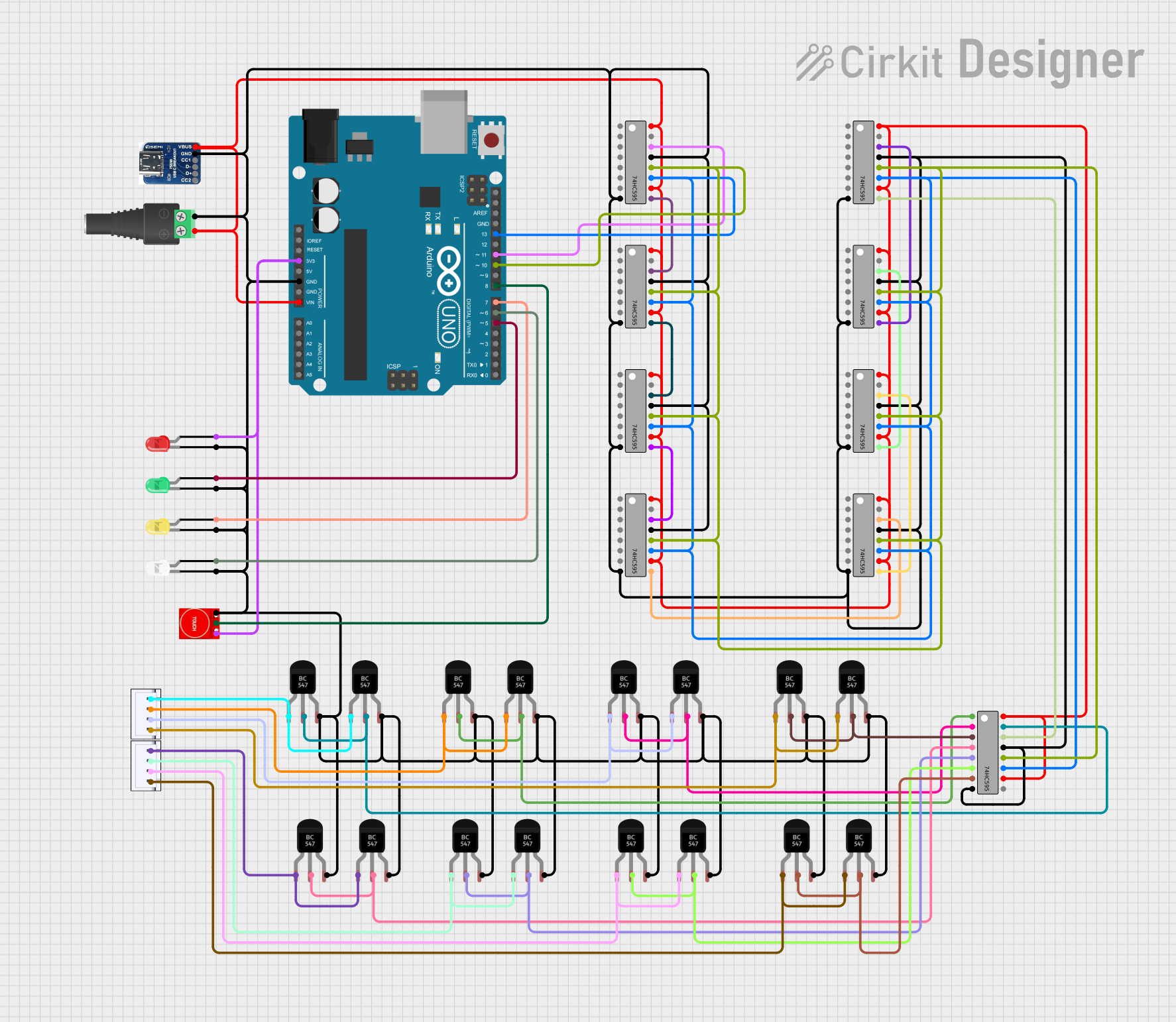 Open Project in Cirkit Designer
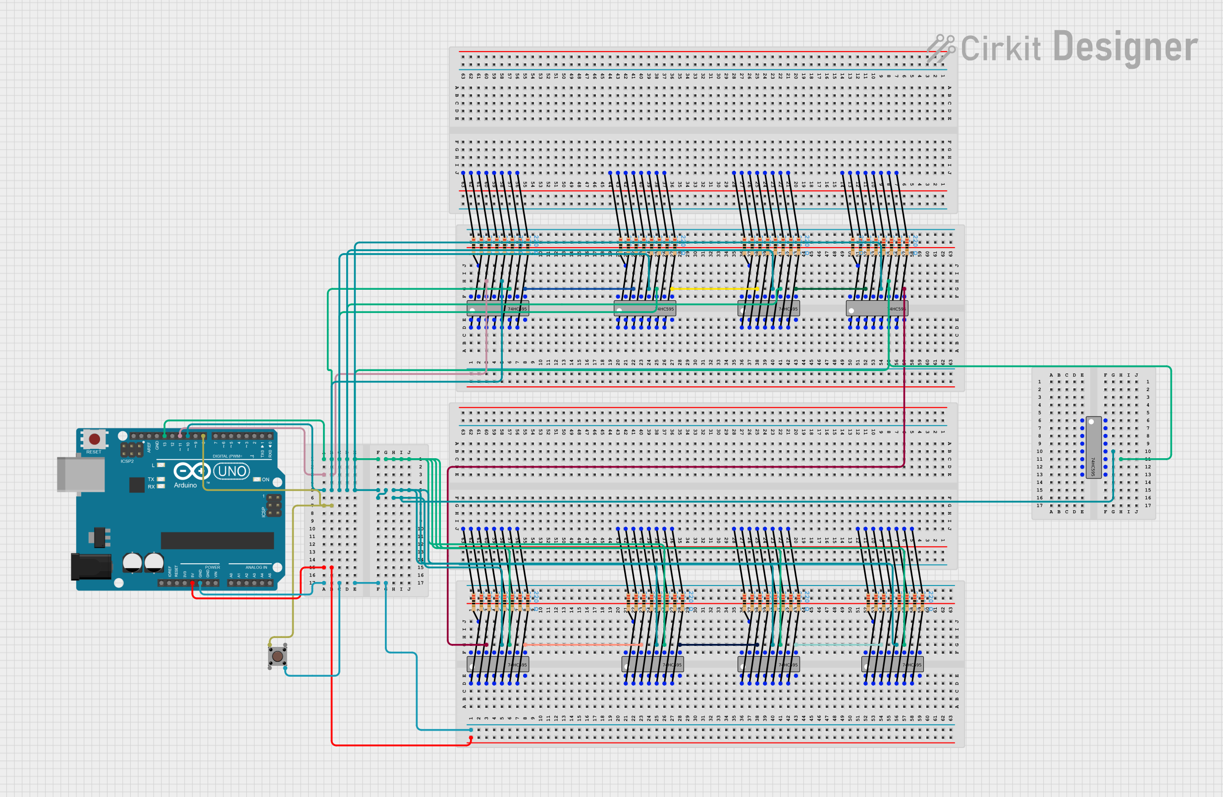 Open Project in Cirkit Designer
 Open Project in Cirkit Designer
Explore Projects Built with 74HC595 SMD
Open Project in Cirkit DesignerOpen Project in Cirkit DesignerOpen Project in Cirkit DesignerOpen Project in Cirkit DesignerCommon Applications
- Driving multiple LEDs or 7-segment displays
- Expanding GPIO pins in microcontroller-based systems
- Controlling relays or other digital devices
- Data storage and transfer in digital systems
Technical Specifications
Key Technical Details
| Parameter | Value |
|---|---|
| Manufacturer | Nexperia |
| Part Number | 74HC595D |
| Supply Voltage (Vcc) | 2V to 6V |
| Maximum Clock Frequency | 25 MHz (at 4.5V to 5.5V Vcc) |
| Output Current per Pin | ±6 mA |
| Maximum Power Dissipation | 500 mW |
| Operating Temperature | -40°C to +125°C |
| Package Type | SMD (SO-16) |
Pin Configuration
The 74HC595D comes in a 16-pin SO (Small Outline) package. Below is the pinout and description:
| Pin No. | Name | Description |
|---|---|---|
| 1 | Q1 | Parallel output 1 |
| 2 | Q2 | Parallel output 2 |
| 3 | Q3 | Parallel output 3 |
| 4 | Q4 | Parallel output 4 |
| 5 | Q5 | Parallel output 5 |
| 6 | Q6 | Parallel output 6 |
| 7 | Q7 | Parallel output 7 |
| 8 | GND | Ground (0V) |
| 9 | Q7' | Serial data output for cascading additional shift registers |
| 10 | MR | Master Reset (active LOW) |
| 11 | SH_CP | Shift register clock input |
| 12 | ST_CP | Storage register clock input (latch pin) |
| 13 | OE | Output enable (active LOW) |
| 14 | DS | Serial data input |
| 15 | Q0 | Parallel output 0 |
| 16 | Vcc | Supply voltage (2V to 6V) |
Usage Instructions
How to Use the 74HC595 in a Circuit
- Power Supply: Connect the Vcc pin (16) to a voltage source (2V to 6V) and the GND pin (8) to ground.
- Data Input: Feed serial data into the DS pin (14). Data is shifted into the register on the rising edge of the SH_CP (11) clock signal.
- Latch Data: Use the ST_CP pin (12) to transfer the data from the shift register to the output latch. A rising edge on ST_CP updates the outputs (Q0-Q7).
- Enable Outputs: Ensure the OE pin (13) is LOW to enable the outputs. If HIGH, the outputs will be in a high-impedance state.
- Cascading: To cascade multiple 74HC595s, connect the Q7' pin (9) of the first IC to the DS pin (14) of the next IC.
Important Considerations
- Use decoupling capacitors (e.g., 0.1 µF) near the Vcc pin to stabilize the power supply.
- Avoid exceeding the maximum current rating of ±6 mA per output pin.
- Ensure proper timing between SH_CP and ST_CP signals to avoid data corruption.
Example: Connecting to an Arduino UNO
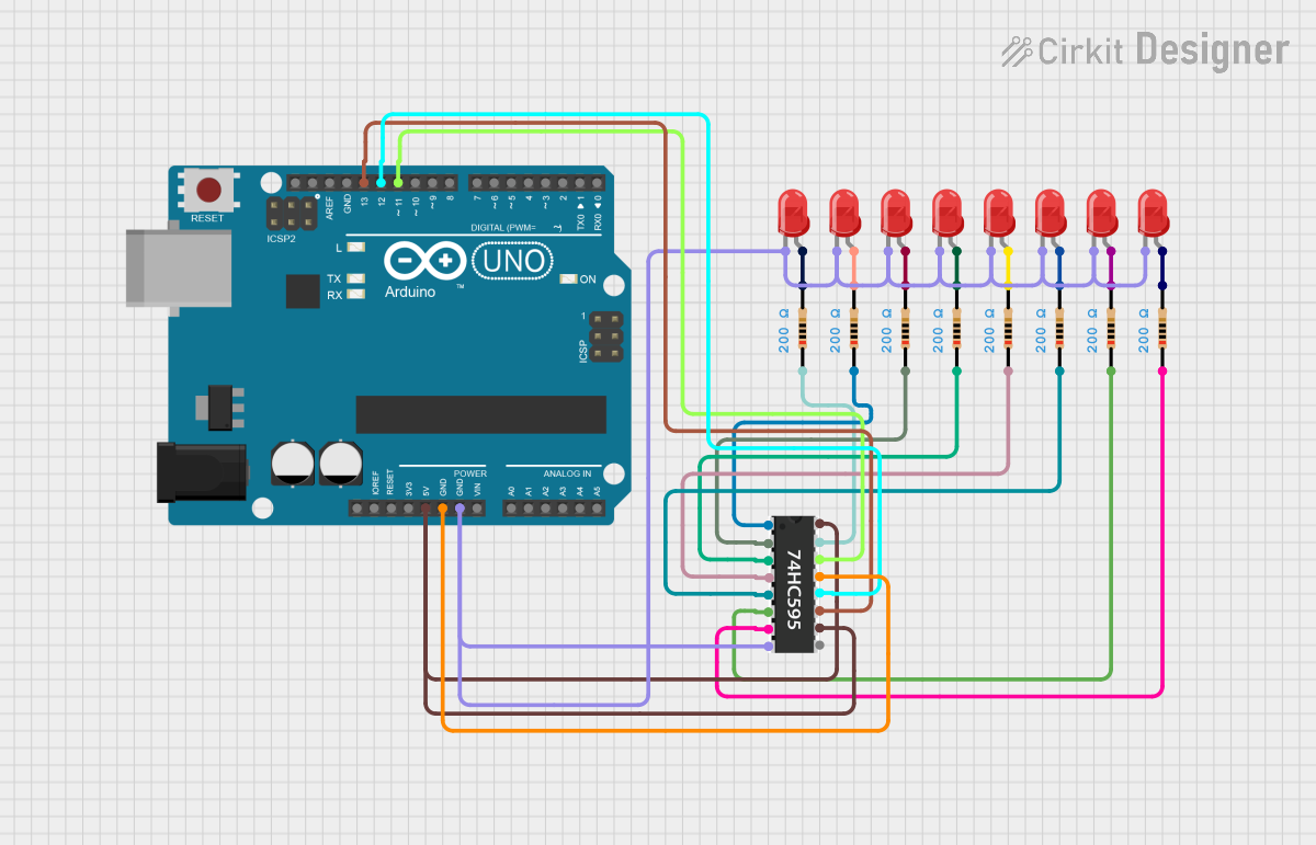
Below is an example of how to control the 74HC595 with an Arduino UNO to light up 8 LEDs.
// Define pins connected to the 74HC595
const int dataPin = 11;  // DS (Serial Data Input)
const int latchPin = 12; // ST_CP (Storage Register Clock)
const int clockPin = 13; // SH_CP (Shift Register Clock)

// Function to send data to the 74HC595
void shiftOutData(byte data) {
  digitalWrite(latchPin, LOW); // Prepare to latch data
  shiftOut(dataPin, clockPin, MSBFIRST, data); // Send data (MSB first)
  digitalWrite(latchPin, HIGH); // Latch data to outputs
}

void setup() {
  pinMode(dataPin, OUTPUT);
  pinMode(latchPin, OUTPUT);
  pinMode(clockPin, OUTPUT);
}

void loop() {
  for (byte i = 0; i < 256; i++) { // Loop through all 8-bit values
    shiftOutData(i); // Send data to the shift register
    delay(200); // Wait 200ms before updating
  }
}
Key Notes for Arduino Users
- Ensure the Arduino's 5V pin is connected to the 74HC595's Vcc pin.
- Use current-limiting resistors (e.g., 220Ω) in series with LEDs to prevent overcurrent.
Troubleshooting and FAQs
Common Issues
Outputs Not Responding:
- Ensure the OE pin (13) is LOW to enable outputs.
- Verify that the ST_CP and SH_CP signals are correctly timed.
Incorrect Output Data:
- Check the data being sent to the DS pin (14).
- Ensure the clock signal (SH_CP) is stable and free of noise.
Cascading Issues:
- Verify the Q7' pin (9) of the first IC is connected to the DS pin (14) of the next IC.
- Ensure the clock and latch signals are shared across all cascaded ICs.
FAQs
Q: Can I use the 74HC595 with a 3.3V microcontroller?
A: Yes, the 74HC595 operates with a supply voltage as low as 2V. Ensure the logic levels of your microcontroller match the IC's input requirements.
Q: How many 74HC595 ICs can I cascade?
A: Theoretically, you can cascade as many as needed, but practical limitations like signal degradation and timing constraints may arise after 8-10 ICs.
Q: What happens if I leave the OE pin floating?
A: The outputs may behave unpredictably. Always tie the OE pin to GND (LOW) to enable outputs or to Vcc (HIGH) to disable them.
By following this documentation, you can effectively integrate the 74HC595D into your projects for efficient pin expansion and control.