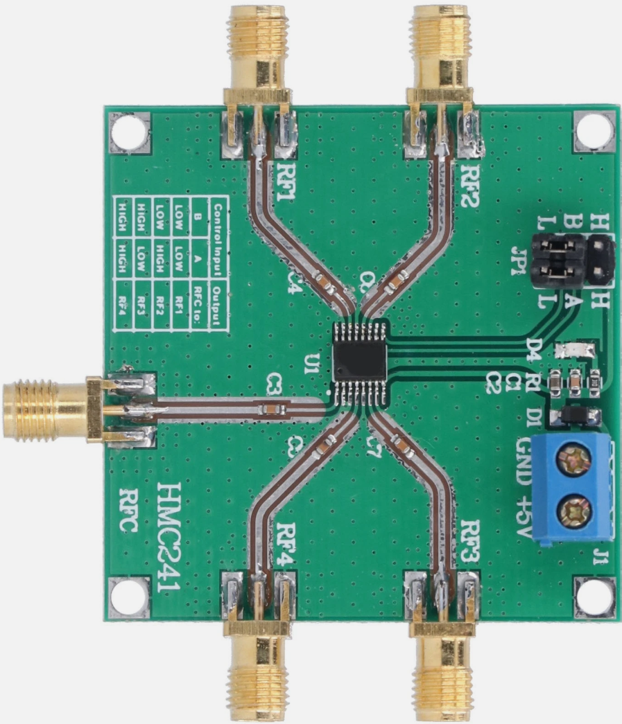
How to Use HMC241 RF Multiplexer: Examples, Pinouts, and Specs
Introduction
The HMC241 is a high-performance RF multiplexer designed for switching RF signals in communication systems. It is widely recognized for its low insertion loss, high isolation, and broad frequency range, making it an ideal choice for applications requiring reliable RF signal routing. This component is commonly used in wireless communication systems, satellite communication, test equipment, and other RF signal processing applications.
Explore Projects Built with HMC241 RF Multiplexer
Explore Projects Built with HMC241 RF Multiplexer
Common Applications:
- Wireless communication systems (e.g., cellular base stations)
- Satellite communication systems
- RF test and measurement equipment
- Signal routing in RF front-end modules
- Radar systems
Technical Specifications
The HMC241 RF multiplexer is designed to meet the demanding requirements of modern RF systems. Below are its key technical specifications:
| Parameter | Value |
|---|---|
| Frequency Range | DC to 3 GHz |
| Insertion Loss | 0.5 dB (typical) |
| Isolation | 40 dB (typical) |
| Input Power Handling | +27 dBm (maximum) |
| Control Voltage Range | 0 V to +5 V |
| Supply Voltage | +5 V |
| Operating Temperature | -40°C to +85°C |
| Package Type | 16-lead SMT package |
Pin Configuration and Descriptions
The HMC241 is housed in a 16-lead surface-mount package. Below is the pin configuration and description:
| Pin Number | Pin Name | Description |
|---|---|---|
| 1 | RF1 | RF input/output port 1 |
| 2 | RF2 | RF input/output port 2 |
| 3 | RF3 | RF input/output port 3 |
| 4 | RF4 | RF input/output port 4 |
| 5 | GND | Ground |
| 6 | VCTL A | Control voltage input A |
| 7 | VCTL B | Control voltage input B |
| 8 | VDD | Supply voltage (+5 V) |
| 9-16 | GND | Ground (multiple pins for improved grounding) |
Usage Instructions
How to Use the HMC241 in a Circuit
- Power Supply: Connect the VDD pin to a stable +5 V power supply. Ensure proper decoupling capacitors are used to minimize noise.
- Grounding: Connect all GND pins to a common ground plane to ensure optimal performance and minimize RF interference.
- Control Signals: Use the VCTL A and VCTL B pins to control the switching state of the multiplexer. These pins accept logic-level signals (0 V or +5 V).
- The combination of VCTL A and VCTL B determines which RF port is active.
- RF Connections: Connect the RF input/output ports (RF1, RF2, RF3, RF4) to the desired RF signal paths. Use high-quality RF connectors and cables to minimize signal loss.
Control Logic Table
The following table shows the control logic for selecting the active RF port:
| VCTL A | VCTL B | Active RF Port |
|---|---|---|
| 0 | 0 | RF1 |
| 0 | 1 | RF2 |
| 1 | 0 | RF3 |
| 1 | 1 | RF4 |
Example Arduino Code
The HMC241 can be controlled using an Arduino UNO to switch between RF ports. Below is an example code snippet:
// Define control pins for the HMC241
const int controlPinA = 2; // Connect to VCTL A
const int controlPinB = 3; // Connect to VCTL B

void setup() {
  // Set control pins as outputs
  pinMode(controlPinA, OUTPUT);
  pinMode(controlPinB, OUTPUT);
}

void loop() {
  // Example: Activate RF1
  digitalWrite(controlPinA, LOW); // Set VCTL A to 0
  digitalWrite(controlPinB, LOW); // Set VCTL B to 0
  delay(1000); // Wait for 1 second

  // Example: Activate RF2
  digitalWrite(controlPinA, LOW); // Set VCTL A to 0
  digitalWrite(controlPinB, HIGH); // Set VCTL B to 1
  delay(1000); // Wait for 1 second

  // Example: Activate RF3
  digitalWrite(controlPinA, HIGH); // Set VCTL A to 1
  digitalWrite(controlPinB, LOW); // Set VCTL B to 0
  delay(1000); // Wait for 1 second

  // Example: Activate RF4
  digitalWrite(controlPinA, HIGH); // Set VCTL A to 1
  digitalWrite(controlPinB, HIGH); // Set VCTL B to 1
  delay(1000); // Wait for 1 second
}
Best Practices
- Use proper RF shielding and grounding techniques to minimize interference.
- Ensure the control signals are clean and free from noise to avoid unintended switching.
- Avoid exceeding the maximum input power rating (+27 dBm) to prevent damage to the component.
Troubleshooting and FAQs
Common Issues and Solutions
No Signal Output:
- Verify that the control signals (VCTL A and VCTL B) are set correctly according to the control logic table.
- Check the power supply voltage on the VDD pin (+5 V).
- Ensure all GND pins are properly connected to the ground plane.
High Insertion Loss:
- Inspect the RF connections for loose or damaged cables.
- Use high-quality RF connectors and minimize the length of RF cables.
Unintended Switching:
- Ensure the control signals are stable and free from noise.
- Add pull-down resistors to the control pins if necessary to prevent floating states.
FAQs
Q1: Can the HMC241 operate at frequencies above 3 GHz?
A1: The HMC241 is optimized for operation up to 3 GHz. Performance may degrade at higher frequencies.
Q2: What type of capacitors should I use for decoupling the power supply?
A2: Use low-ESR ceramic capacitors (e.g., 0.1 µF and 10 µF) close to the VDD pin for effective decoupling.
Q3: Can I use a 3.3 V control signal for VCTL A and VCTL B?
A3: No, the control signals must be within the specified range of 0 V to +5 V for proper operation.
Q4: Is the HMC241 suitable for high-power RF applications?
A4: The HMC241 can handle input power up to +27 dBm. For higher power levels, consider using a different multiplexer with a higher power rating.