How to Use Terminal 2 PCB Verde: Examples, Pinouts, and Specs
Introduction
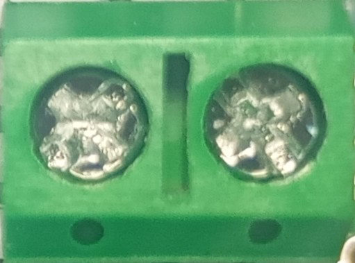
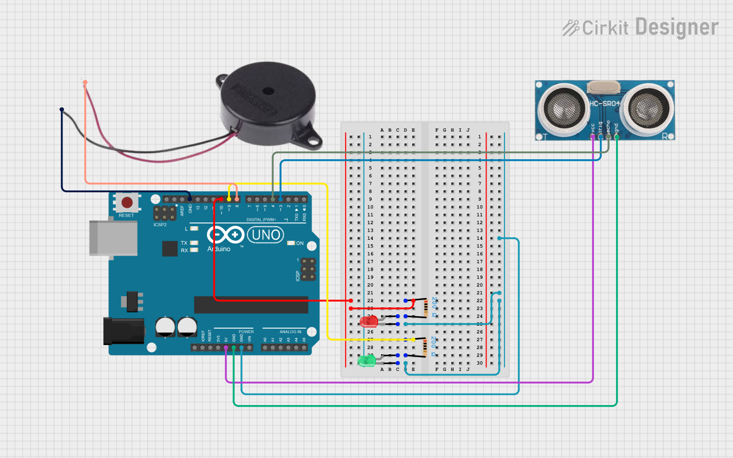
The Terminal 2 PCB Verde is a printed circuit board (PCB) designed for connecting and organizing electrical components in a compact and efficient manner. It features a green solder mask, which not only enhances visibility during assembly but also provides protection against environmental factors such as moisture and dust. This PCB is ideal for prototyping, small-scale production, and educational purposes.
Explore Projects Built with Terminal 2 PCB Verde
Explore Projects Built with Terminal 2 PCB Verde
Common Applications and Use Cases
- Prototyping and testing electronic circuits
- Educational projects for learning PCB design and assembly
- Small-scale production of electronic devices
- DIY electronics and hobbyist projects
- Organizing and connecting components in a structured layout
Technical Specifications
The Terminal 2 PCB Verde is designed to meet the needs of a wide range of electronic applications. Below are its key technical details:
General Specifications
| Parameter | Value |
|---|---|
| Material | FR4 (Flame Retardant 4) |
| Solder Mask Color | Green |
| PCB Thickness | 1.6 mm |
| Copper Layer Thickness | 1 oz/ft² (35 µm) |
| Dimensions | 100 mm x 80 mm |
| Number of Layers | 2 |
| Operating Temperature | -40°C to 85°C |
| Surface Finish | HASL (Hot Air Solder Leveling) |
Pin Configuration and Descriptions
The Terminal 2 PCB Verde does not have predefined pins but includes a grid of plated through-holes (PTH) for component mounting and soldering. Below is a description of its layout:
| Feature | Description |
|---|---|
| Plated Through-Holes | Standard 1.0 mm diameter holes for mounting components and soldering wires. |
| Power Rails | Dedicated tracks for VCC and GND to simplify power distribution. |
| Mounting Holes | Four 3.2 mm holes for securing the PCB to an enclosure or surface. |
| Silkscreen Markings | Labels for component placement and orientation. |
Usage Instructions
The Terminal 2 PCB Verde is straightforward to use and can be adapted for various electronic projects. Follow the steps below to integrate it into your circuit:
Step-by-Step Instructions
- Design Your Circuit: Plan your circuit layout, including the placement of components and connections.
- Prepare Components: Gather all necessary components, such as resistors, capacitors, ICs, and connectors.
- Place Components: Insert the components into the plated through-holes according to your design.
- Solder Components: Use a soldering iron and solder wire to secure the components to the PCB. Ensure proper solder joints to avoid cold soldering.
- Connect Power and Ground: Use the dedicated power rails for VCC and GND connections to simplify wiring.
- Test the Circuit: Verify the functionality of your circuit using a multimeter or oscilloscope before finalizing the assembly.
Important Considerations and Best Practices
- Avoid Overheating: Excessive heat during soldering can damage the PCB or components. Use a temperature-controlled soldering iron.
- Clean the PCB: After soldering, clean the PCB with isopropyl alcohol to remove flux residues.
- Use Proper Tools: Use a PCB holder or vise to keep the board steady during soldering.
- Double-Check Connections: Verify all connections before powering the circuit to prevent short circuits or component damage.
Example: Connecting to an Arduino UNO
The Terminal 2 PCB Verde can be used to create custom shields or breakout boards for an Arduino UNO. Below is an example of connecting an LED and a resistor to an Arduino using the PCB:
// Example code for blinking an LED connected via the Terminal 2 PCB Verde
// Connect the LED's anode to pin 13 and cathode to GND through a 220-ohm resistor.

void setup() {
  pinMode(13, OUTPUT); // Set pin 13 as an output
}

void loop() {
  digitalWrite(13, HIGH); // Turn the LED on
  delay(1000);            // Wait for 1 second
  digitalWrite(13, LOW);  // Turn the LED off
  delay(1000);            // Wait for 1 second
}
Troubleshooting and FAQs
Common Issues and Solutions
Issue: Components are not functioning as expected.
- Solution: Check for cold solder joints or incorrect component placement. Re-solder if necessary.
Issue: Short circuits on the PCB.
- Solution: Inspect the solder joints for bridges between adjacent pads. Use a solder wick or desoldering pump to remove excess solder.
Issue: PCB traces are damaged during soldering.
- Solution: Avoid applying excessive heat. If a trace is damaged, use a jumper wire to restore the connection.
Issue: Power distribution is inconsistent.
- Solution: Ensure proper connections to the VCC and GND rails. Verify the power source voltage and current ratings.
FAQs
Q: Can the Terminal 2 PCB Verde handle high-power components?
A: The PCB is designed for low to moderate power applications. For high-power components, ensure proper heat dissipation and use thicker traces or external wiring.
Q: Is the PCB reusable after desoldering components?
A: Yes, the PCB can be reused if components are carefully desoldered without damaging the plated through-holes or traces.
Q: Can I cut the PCB to a smaller size?
A: Yes, the PCB can be cut using a PCB cutter or a rotary tool. However, ensure that the cut does not damage critical traces or components.
This concludes the documentation for the Terminal 2 PCB Verde.