How to Use CD4013: Examples, Pinouts, and Specs
Introduction
The CD4013 is a dual D-type flip-flop integrated circuit (IC) manufactured under the part ID CD4013. It contains two independent flip-flops, each with its own data (D) input, clock (CLK) input, set (SET), reset (RESET), and complementary outputs (Q and Q̅). This IC is widely used in digital electronics for data storage, transfer, and synchronization tasks.
Explore Projects Built with CD4013
Explore Projects Built with CD4013
Common Applications
- Data storage and latching
- Frequency division and counters
- Shift registers
- Memory elements in digital systems
- Signal synchronization and debouncing
Technical Specifications
The CD4013 is a versatile IC with the following key technical details:
| Parameter | Value |
|---|---|
| Supply Voltage (VDD) | 3V to 15V |
| Input Voltage Range | 0V to VDD |
| Maximum Clock Frequency | 3 MHz (at VDD = 15V) |
| Propagation Delay | 200 ns (typical at VDD = 10V) |
| Power Dissipation | 500 mW (maximum) |
| Operating Temperature | -55°C to +125°C |
| Package Types | DIP-14, SOIC-14, TSSOP-14 |
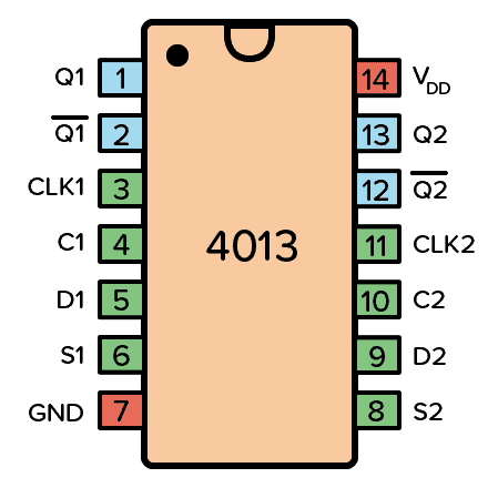
Pin Configuration and Descriptions
The CD4013 is a 14-pin IC. The pinout and descriptions are as follows:
| Pin Number | Pin Name | Description |
|---|---|---|
| 1 | Q1 | Output of Flip-Flop 1 |
| 2 | Q̅1 | Complementary Output of Flip-Flop 1 |
| 3 | CLK1 | Clock Input for Flip-Flop 1 |
| 4 | D1 | Data Input for Flip-Flop 1 |
| 5 | RESET1 | Reset Input for Flip-Flop 1 (Active HIGH) |
| 6 | SET1 | Set Input for Flip-Flop 1 (Active HIGH) |
| 7 | GND | Ground (0V) |
| 8 | SET2 | Set Input for Flip-Flop 2 (Active HIGH) |
| 9 | RESET2 | Reset Input for Flip-Flop 2 (Active HIGH) |
| 10 | D2 | Data Input for Flip-Flop 2 |
| 11 | CLK2 | Clock Input for Flip-Flop 2 |
| 12 | Q̅2 | Complementary Output of Flip-Flop 2 |
| 13 | Q2 | Output of Flip-Flop 2 |
| 14 | VDD | Positive Supply Voltage |
Usage Instructions
The CD4013 is straightforward to use in digital circuits. Below are the steps and considerations for its implementation:
Basic Circuit Connection
- Power Supply: Connect pin 14 (VDD) to the positive supply voltage (3V to 15V) and pin 7 (GND) to ground.
- Inputs: Provide the desired logic signals to the D, CLK, SET, and RESET pins of the flip-flops.
- Outputs: Use the Q and Q̅ pins to retrieve the stored or processed data.
Important Considerations
- SET and RESET: These inputs are active HIGH. If both are HIGH simultaneously, the behavior is undefined. Ensure only one is active at a time.
- Clock Signal: The flip-flop changes state on the rising edge of the clock signal.
- Unused Inputs: Tie unused inputs (e.g., SET, RESET, or D) to a defined logic level (VDD or GND) to avoid floating inputs, which can cause erratic behavior.
- Bypass Capacitor: Place a 0.1 µF decoupling capacitor between VDD and GND to filter noise.
Example: Using CD4013 with Arduino UNO
The CD4013 can be used with an Arduino UNO to create a simple toggle flip-flop circuit. Below is an example code to demonstrate this:
// Example: Using CD4013 with Arduino UNO
// This code toggles the state of a flip-flop on each button press.

const int clockPin = 3;  // Arduino pin connected to CD4013 CLK input
const int dataPin = 4;   // Arduino pin connected to CD4013 D input
const int buttonPin = 2; // Button input pin

int buttonState = 0;     // Variable to store button state
int lastButtonState = 0; // Variable to store last button state

void setup() {
  pinMode(clockPin, OUTPUT); // Set clock pin as output
  pinMode(dataPin, OUTPUT);  // Set data pin as output
  pinMode(buttonPin, INPUT); // Set button pin as input
}

void loop() {
  buttonState = digitalRead(buttonPin); // Read the button state

  // Check if the button is pressed (and released) to toggle the flip-flop
  if (buttonState == HIGH && lastButtonState == LOW) {
    digitalWrite(dataPin, HIGH);  // Set D input HIGH
    digitalWrite(clockPin, HIGH); // Generate a rising edge on CLK
    delay(10);                    // Short delay for stability
    digitalWrite(clockPin, LOW);  // Set CLK LOW
    digitalWrite(dataPin, LOW);   // Reset D input to LOW
  }

  lastButtonState = buttonState; // Update the last button state
}
Notes:
- Ensure the CD4013 is powered within its voltage range (3V to 15V).
- Use pull-down resistors on the button input to avoid floating states.
Troubleshooting and FAQs
Common Issues
Flip-Flop Not Responding to Clock Signal:
- Ensure the clock signal has a clean rising edge.
- Verify that the clock frequency is within the IC's maximum limit.
Unexpected Behavior:
- Check for floating inputs. Tie unused inputs to VDD or GND.
- Ensure SET and RESET are not activated simultaneously.
No Output Signal:
- Verify the power supply connections (VDD and GND).
- Check the input signals for proper logic levels.
FAQs
Q1: Can the CD4013 operate at 5V?
Yes, the CD4013 can operate at 5V, which is within its supply voltage range (3V to 15V).
Q2: What happens if both SET and RESET are HIGH?
The behavior is undefined. Avoid activating both inputs simultaneously.
Q3: Can the CD4013 be used for frequency division?
Yes, the CD4013 can divide the frequency of a clock signal by 2 using a single flip-flop.
Q4: How do I debounce a button using the CD4013?
You can use the CD4013 to latch the button state and eliminate bouncing by connecting the button to the clock input and using the Q output as the debounced signal.
By following the guidelines and examples provided, you can effectively use the CD4013 in a variety of digital applications.