How to Use ADS1256: Examples, Pinouts, and Specs
Introduction
The ADS1256, manufactured by Texas Instruments, is a high-performance 24-bit analog-to-digital converter (ADC) with a high-speed serial interface. It is designed for precision measurement applications, offering exceptional resolution, low noise, and versatile input configurations. The ADS1256 features an integrated programmable gain amplifier (PGA), multiple input channels, and a flexible data rate, making it ideal for applications requiring accurate and reliable data acquisition.
Explore Projects Built with ADS1256
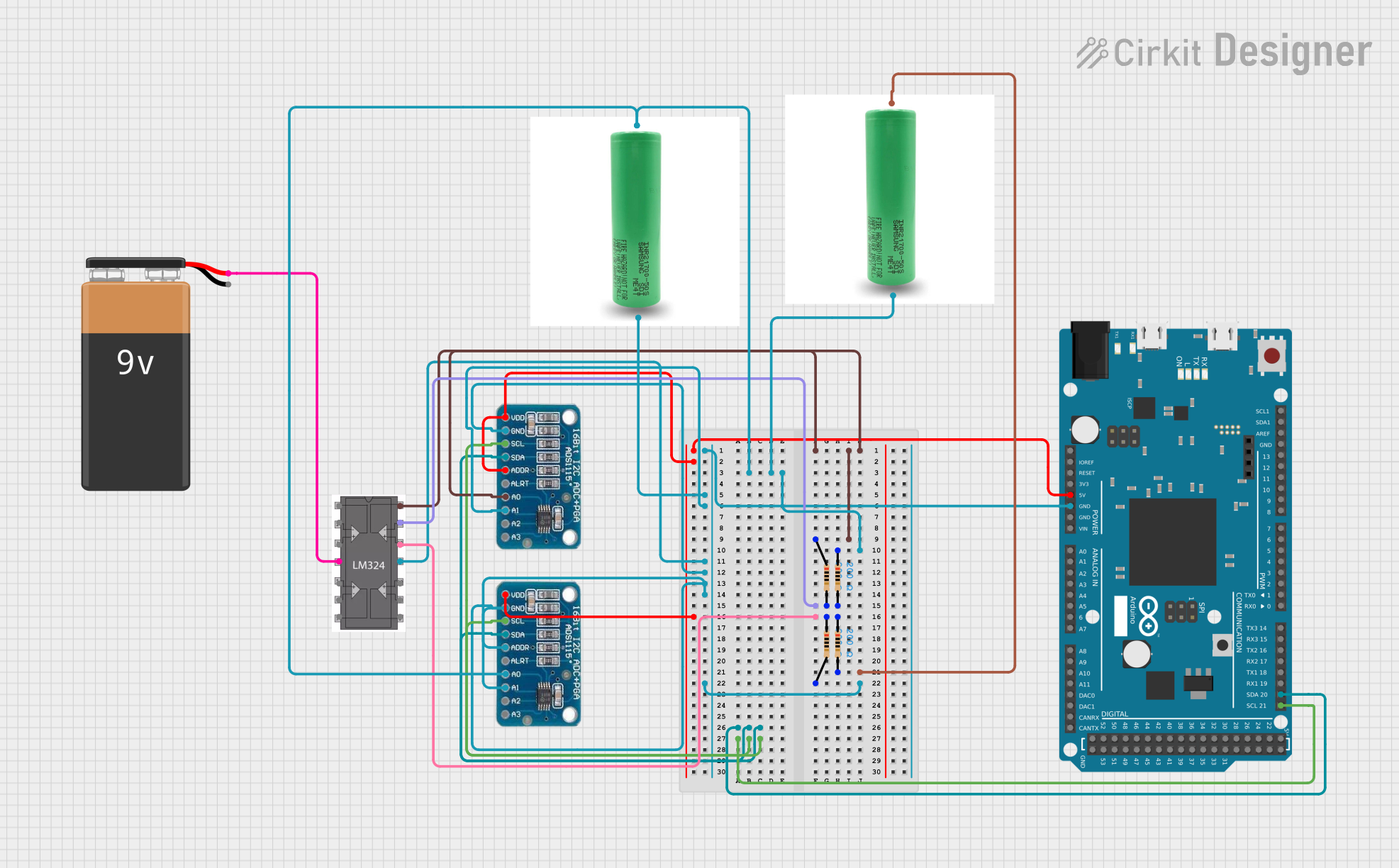
Explore Projects Built with ADS1256
Common Applications
- Industrial automation and control systems
- Medical instrumentation and diagnostic devices
- Sensor data acquisition (e.g., temperature, pressure, and strain gauges)
- Weighing scales and precision measurement systems
- Energy monitoring and metering
Technical Specifications
Key Technical Details
| Parameter | Value |
|---|---|
| Resolution | 24-bit |
| Number of Input Channels | 8 single-ended or 4 differential |
| Input Voltage Range | ±2.5V (default, with internal reference) |
| Programmable Gain Options | 1, 2, 4, 8, 16, 32, 64 |
| Data Rate | 2.5 SPS to 30,000 SPS |
| Interface | SPI (Serial Peripheral Interface) |
| Supply Voltage | 2.7V to 5.25V |
| Power Consumption | 21mW (typical at 5V supply) |
| Operating Temperature Range | -40°C to +85°C |
Pin Configuration and Descriptions
The ADS1256 is typically available in a 28-pin TSSOP package. Below is the pin configuration:
| Pin Number | Pin Name | Description |
|---|---|---|
| 1 | VREFP | Positive reference voltage input |
| 2 | VREFN | Negative reference voltage input |
| 3 | AIN0 | Analog input channel 0 |
| 4 | AIN1 | Analog input channel 1 |
| 5 | AIN2 | Analog input channel 2 |
| 6 | AIN3 | Analog input channel 3 |
| 7 | AIN4 | Analog input channel 4 |
| 8 | AIN5 | Analog input channel 5 |
| 9 | AIN6 | Analog input channel 6 |
| 10 | AIN7 | Analog input channel 7 |
| 11 | AGND | Analog ground |
| 12 | DGND | Digital ground |
| 13 | DVDD | Digital supply voltage |
| 14 | AVDD | Analog supply voltage |
| 15 | CLKIN | External clock input |
| 16 | CLKOUT | Clock output |
| 17 | DRDY | Data ready output (active low) |
| 18 | CS | Chip select input (active low) |
| 19 | DIN | SPI data input |
| 20 | DOUT | SPI data output |
| 21 | SCLK | SPI clock input |
| 22 | RESET | Reset input (active low) |
| 23-28 | NC | No connection |
Usage Instructions
How to Use the ADS1256 in a Circuit
- Power Supply: Connect the analog (AVDD) and digital (DVDD) supply pins to a stable voltage source within the specified range (2.7V to 5.25V). Ensure proper decoupling capacitors are placed close to the supply pins.
- Reference Voltage: Provide a stable reference voltage to the VREFP and VREFN pins. The internal reference can also be used for simplicity.
- Input Configuration: Connect the analog input signals to the AINx pins. Configure the inputs as single-ended or differential based on your application.
- SPI Communication: Connect the SPI interface pins (CS, DIN, DOUT, SCLK) to a microcontroller or processor. Ensure proper pull-up or pull-down resistors are used as needed.
- Clock Source: Provide an external clock signal to the CLKIN pin or use the internal oscillator.
- Data Acquisition: Monitor the DRDY pin to detect when new data is available. Use SPI commands to read the converted data from the DOUT pin.
Important Considerations and Best Practices
- Use low-noise power supplies and proper grounding techniques to minimize noise and interference.
- Place decoupling capacitors (e.g., 0.1µF and 10µF) close to the power supply pins.
- Avoid long traces for analog input signals to reduce noise pickup.
- Configure the PGA gain and data rate based on the input signal characteristics and desired resolution.
- Ensure the SPI clock frequency does not exceed the maximum specified in the datasheet.
Example Code for Arduino UNO
Below is an example of how to interface the ADS1256 with an Arduino UNO using SPI:
#include <SPI.h>

// Pin definitions
#define CS_PIN 10  // Chip select pin
#define DRDY_PIN 9 // Data ready pin

void setup() {
  pinMode(CS_PIN, OUTPUT);
  pinMode(DRDY_PIN, INPUT);
  digitalWrite(CS_PIN, HIGH); // Set CS high initially

  SPI.begin(); // Initialize SPI
  SPI.setDataMode(SPI_MODE1); // ADS1256 uses SPI mode 1
  SPI.setClockDivider(SPI_CLOCK_DIV16); // Set SPI clock speed
  Serial.begin(9600); // Initialize serial communication
}

void loop() {
  if (digitalRead(DRDY_PIN) == LOW) { // Check if data is ready
    digitalWrite(CS_PIN, LOW); // Select the ADS1256
    byte command = 0x01; // Example command to read data
    SPI.transfer(command); // Send command
    byte dataHigh = SPI.transfer(0x00); // Read high byte
    byte dataMid = SPI.transfer(0x00); // Read middle byte
    byte dataLow = SPI.transfer(0x00); // Read low byte
    digitalWrite(CS_PIN, HIGH); // Deselect the ADS1256

    // Combine the bytes into a 24-bit value
    long result = ((long)dataHigh << 16) | ((long)dataMid << 8) | dataLow;
    Serial.println(result); // Print the result
  }
}
Troubleshooting and FAQs
Common Issues and Solutions
No Data Output:
- Ensure the SPI connections (CS, DIN, DOUT, SCLK) are correctly wired.
- Verify that the DRDY pin is monitored to detect when data is ready.
- Check the power supply and reference voltage connections.
Noisy or Inaccurate Readings:
- Use proper grounding and shielding to minimize noise.
- Verify that the input signals are within the specified voltage range.
- Ensure the PGA gain and data rate are configured appropriately.
Device Not Responding:
- Confirm that the CS pin is pulled low during SPI communication.
- Check the SPI clock frequency and mode settings.
FAQs
Q: Can I use the ADS1256 with a 3.3V microcontroller?
A: Yes, the ADS1256 supports a supply voltage range of 2.7V to 5.25V, making it compatible with 3.3V systems.
Q: What is the maximum sampling rate of the ADS1256?
A: The ADS1256 supports a maximum data rate of 30,000 samples per second (SPS).
Q: Can I use the internal reference voltage?
A: Yes, the ADS1256 includes an internal reference voltage, but for higher accuracy, an external reference is recommended.