
How to Use 20x50 PCB2: Examples, Pinouts, and Specs
 Design with 20x50 PCB2 in Cirkit Designer
Introduction
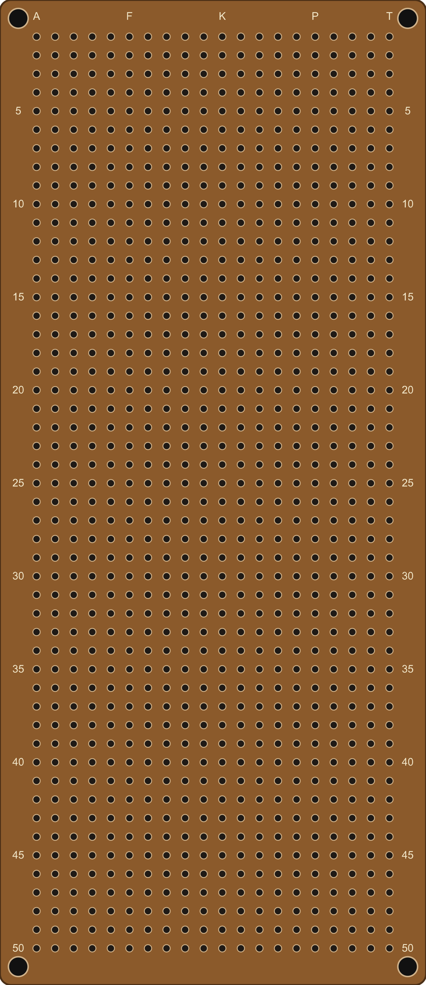
The 20x50 PCB2 is a compact printed circuit board (PCB) with dimensions of 20 mm by 50 mm. It is designed to serve as a versatile platform for mounting electronic components and establishing electrical connections between them. This PCB is ideal for prototyping, small-scale projects, and custom circuit designs where space is a constraint. Its standardized layout and high-quality construction make it suitable for both hobbyists and professional engineers.
Explore Projects Built with 20x50 PCB2
 Open Project in Cirkit Designer
 Open Project in Cirkit Designer
 Open Project in Cirkit Designer
 Open Project in Cirkit Designer
Explore Projects Built with 20x50 PCB2
Open Project in Cirkit DesignerOpen Project in Cirkit DesignerOpen Project in Cirkit DesignerOpen Project in Cirkit DesignerCommon Applications and Use Cases
- Prototyping small electronic circuits
- Building compact IoT devices
- Custom sensor modules
- Educational projects and DIY electronics
- Space-constrained embedded systems
Technical Specifications
The 20x50 PCB2 is designed to meet the needs of compact and efficient circuit designs. Below are its key technical details:
General Specifications
| Parameter | Value |
|---|---|
| Dimensions | 20 mm x 50 mm |
| Material | FR4 (Flame Retardant 4) |
| Thickness | 1.6 mm |
| Copper Layer Thickness | 35 µm (1 oz/ft²) |
| Number of Layers | Single-layer or double-layer (varies by model) |
| Hole Diameter | 1.0 mm |
| Hole Pitch | 2.54 mm (standard grid) |
| Surface Finish | HASL (Hot Air Solder Leveling) or ENIG (Electroless Nickel Immersion Gold) |
| Solder Mask Color | Green (default) |
| Silkscreen Color | White |
Pin Configuration and Descriptions
The 20x50 PCB2 does not have predefined pins but features a grid of plated through-holes (PTH) for component mounting. Below is a description of the hole layout:
| Feature | Description |
|---|---|
| Plated Through-Holes | 1.0 mm diameter holes for mounting components or headers. |
| Grid Layout | Standard 2.54 mm pitch for compatibility with DIP components, headers, and connectors. |
| Edge Pads (optional) | Some models include edge pads for external connections. |
Usage Instructions
The 20x50 PCB2 is straightforward to use and can be adapted for a wide range of applications. Follow the steps below to integrate it into your project:
Step 1: Plan Your Circuit
- Sketch your circuit design on paper or use PCB design software to map out component placement.
- Ensure that the components fit within the 20x50 mm area and align with the 2.54 mm grid.
Step 2: Mount Components
- Insert components (e.g., resistors, capacitors, ICs) into the plated through-holes.
- Ensure proper orientation for polarized components like diodes and electrolytic capacitors.
Step 3: Solder Connections
- Use a soldering iron to securely solder the component leads to the copper pads.
- Trim excess leads with wire cutters after soldering.
Step 4: Add External Connections
- Use headers, wires, or connectors to interface the PCB with other parts of your circuit.
- For Arduino UNO users, you can solder male headers to the PCB and use jumper wires to connect it to the Arduino.
Step 5: Test Your Circuit
- Verify all connections with a multimeter before powering the circuit.
- Power the circuit and test its functionality.
Example: Connecting to an Arduino UNO
Below is an example of how to use the 20x50 PCB2 to create a simple LED circuit controlled by an Arduino UNO:
Circuit Description
- An LED is connected to digital pin 13 of the Arduino UNO through a 220-ohm resistor.
- The circuit is built on the 20x50 PCB2.
Arduino Code
// Simple LED Blink Example
// This code blinks an LED connected to pin 13 of the Arduino UNO.

// Define the LED pin
const int ledPin = 13;

void setup() {
  // Set the LED pin as an output
  pinMode(ledPin, OUTPUT);
}

void loop() {
  // Turn the LED on
  digitalWrite(ledPin, HIGH);
  delay(1000); // Wait for 1 second

  // Turn the LED off
  digitalWrite(ledPin, LOW);
  delay(1000); // Wait for 1 second
}
Best Practices
- Use flux to ensure clean and reliable solder joints.
- Avoid overheating the PCB during soldering to prevent damage to the copper traces.
- Label components on the silkscreen layer for easier debugging and maintenance.
Troubleshooting and FAQs
Common Issues
Cold Solder Joints
- Cause: Insufficient heat or solder during soldering.
- Solution: Reheat the joint and apply more solder to ensure a solid connection.
Short Circuits
- Cause: Solder bridges between adjacent pads or traces.
- Solution: Use a solder wick or desoldering pump to remove excess solder.
Component Misalignment
- Cause: Incorrect placement of components on the grid.
- Solution: Double-check the layout before soldering and use a breadboard for prototyping.
Damaged Traces
- Cause: Excessive heat or mechanical stress.
- Solution: Repair damaged traces with a thin wire or conductive ink.
FAQs
Q: Can I use the 20x50 PCB2 for high-frequency circuits?
A: Yes, but ensure proper grounding and trace design to minimize interference.
Q: Is the PCB compatible with surface-mount components?
A: The 20x50 PCB2 is primarily designed for through-hole components, but surface-mount components can be used with careful soldering.
Q: Can I cut the PCB to a smaller size?
A: Yes, the PCB can be cut using a PCB cutter or a fine saw, but ensure that the cut does not damage critical traces or components.
Q: What is the maximum current the PCB can handle?
A: The current capacity depends on the trace width and copper thickness. For standard 35 µm copper, refer to IPC-2221 standards for trace current ratings.
By following this documentation, you can effectively use the 20x50 PCB2 for your electronic projects.