
How to Use 25LC040: Examples, Pinouts, and Specs
 Design with 25LC040 in Cirkit Designer
Introduction
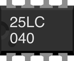
The 25LC040 is a 4 Kbit (512 x 8) serial EEPROM manufactured by Microchip Technology. It is designed for non-volatile data storage, meaning it retains data even when power is removed. The component communicates using the Serial Peripheral Interface (SPI) protocol, making it suitable for a wide range of embedded systems and microcontroller-based applications.
Explore Projects Built with 25LC040
 Open Project in Cirkit Designer
 Open Project in Cirkit Designer
 Open Project in Cirkit Designer
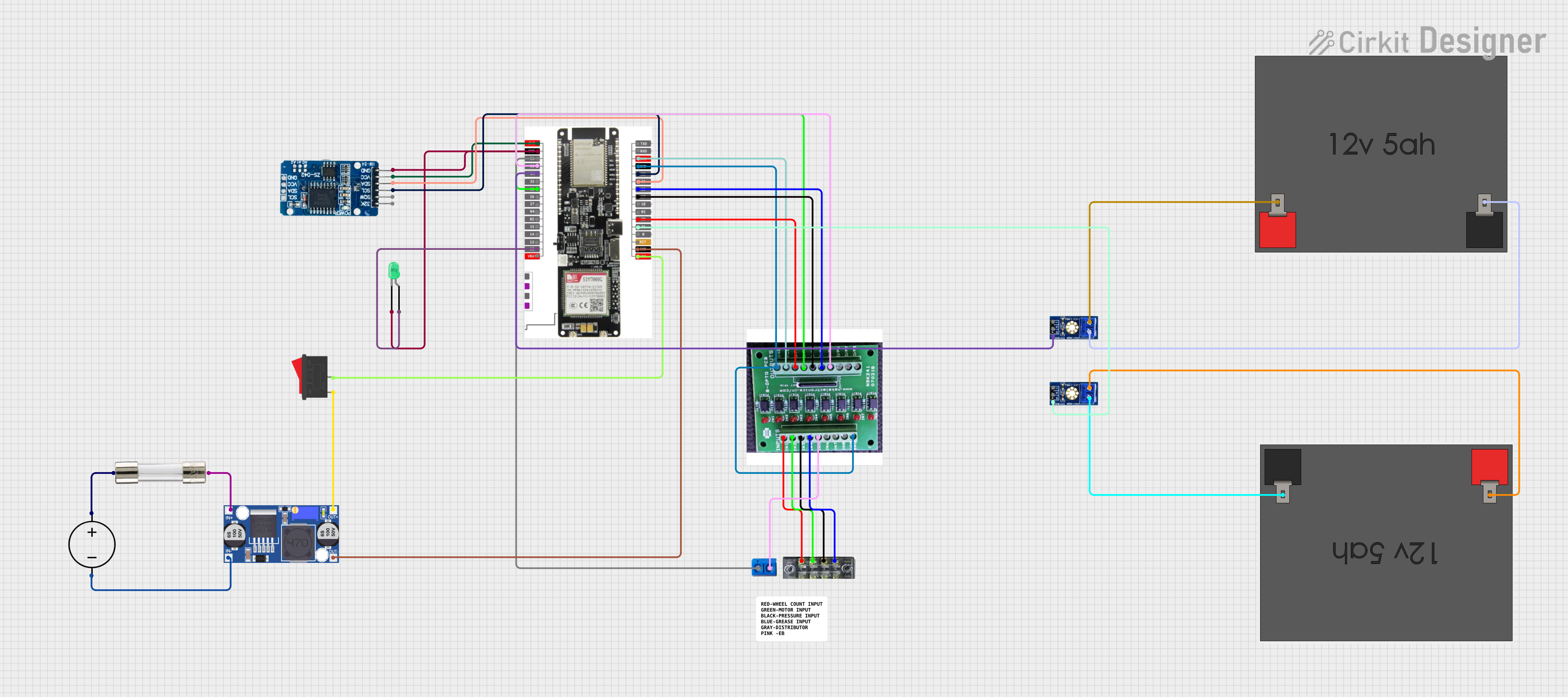 Open Project in Cirkit Designer
Explore Projects Built with 25LC040
Open Project in Cirkit DesignerOpen Project in Cirkit DesignerOpen Project in Cirkit DesignerOpen Project in Cirkit DesignerCommon Applications and Use Cases
- Configuration data storage in embedded systems
- Calibration data storage for sensors
- Non-volatile memory for microcontroller projects
- Data logging in IoT devices
- Storing lookup tables or small databases
Technical Specifications
The following table outlines the key technical details of the 25LC040:
| Parameter | Value |
|---|---|
| Memory Size | 4 Kbit (512 x 8) |
| Interface Protocol | SPI (Serial Peripheral Interface) |
| Operating Voltage Range | 2.5V to 5.5V |
| Maximum Clock Frequency | 10 MHz (at 4.5V to 5.5V) |
| Write Cycle Time | 5 ms (typical) |
| Endurance | 1,000,000 write cycles |
| Data Retention | 200 years |
| Operating Temperature | -40°C to +85°C |
| Package Types | PDIP, SOIC, TSSOP, MSOP |
Pin Configuration and Descriptions
The 25LC040 is typically available in an 8-pin package. The pinout and descriptions are as follows:
| Pin No. | Pin Name | Description |
|---|---|---|
| 1 | CS | Chip Select: Activates the device when pulled low. |
| 2 | SO | Serial Data Output: Outputs data to the SPI master. |
| 3 | WP | Write Protect: Disables write operations when pulled high. |
| 4 | VSS | Ground: Connect to system ground. |
| 5 | SI | Serial Data Input: Receives data from the SPI master. |
| 6 | SCK | Serial Clock: Clock signal for SPI communication. |
| 7 | HOLD | Hold: Pauses communication when pulled low (optional). |
| 8 | VCC | Power Supply: Connect to a voltage source (2.5V to 5.5V). |
Usage Instructions
How to Use the 25LC040 in a Circuit
- Power Supply: Connect the VCC pin to a power source (2.5V to 5.5V) and the VSS pin to ground.
- SPI Connections:
- Connect the CS pin to a GPIO pin on the microcontroller to enable/disable the chip.
- Connect the SCK pin to the SPI clock pin of the microcontroller.
- Connect the SI pin to the SPI MOSI (Master Out Slave In) pin.
- Connect the SO pin to the SPI MISO (Master In Slave Out) pin.
- Optional Pins:
- If write protection is required, pull the WP pin high.
- If the hold function is needed, connect the HOLD pin to a GPIO pin or pull it high if unused.
- SPI Configuration: Configure the SPI interface on the microcontroller with the following settings:
- Clock polarity (CPOL): 0
- Clock phase (CPHA): 0
- Data order: MSB first
- Data Communication:
- To write data, send the WRITE instruction (0x02) followed by the memory address and data byte(s).
- To read data, send the READ instruction (0x03) followed by the memory address and read the data byte(s) from the SO pin.
Important Considerations and Best Practices
- Write Protection: Use the WP pin to prevent accidental writes to the memory.
- Timing: Ensure proper timing for SPI signals, especially the clock frequency, to avoid communication errors.
- Pull-Up Resistors: Use pull-up resistors on the CS, WP, and HOLD pins if they are not actively driven by the microcontroller.
- Write Cycle Time: Allow sufficient time (5 ms) for write operations to complete before initiating another write.
Example Code for Arduino UNO
Below is an example of how to interface the 25LC040 with an Arduino UNO using the SPI library:
#include <SPI.h>

// Pin definitions
const int CS_PIN = 10; // Chip Select pin connected to Arduino pin 10

void setup() {
  // Initialize SPI and Chip Select pin
  SPI.begin();
  pinMode(CS_PIN, OUTPUT);
  digitalWrite(CS_PIN, HIGH); // Deselect the chip
  Serial.begin(9600);
}

void loop() {
  // Example: Write and read a byte from the 25LC040
  byte address = 0x00; // Memory address to write to
  byte dataToWrite = 0x55; // Example data to write
  byte readData;

  // Write data to the EEPROM
  writeEEPROM(address, dataToWrite);

  // Read data back from the EEPROM
  readData = readEEPROM(address);

  // Print the read data to the Serial Monitor
  Serial.print("Read Data: 0x");
  Serial.println(readData, HEX);

  delay(1000); // Wait for 1 second
}

void writeEEPROM(byte address, byte data) {
  digitalWrite(CS_PIN, LOW); // Select the chip
  SPI.transfer(0x02); // Send WRITE instruction
  SPI.transfer(address); // Send memory address
  SPI.transfer(data); // Send data byte
  digitalWrite(CS_PIN, HIGH); // Deselect the chip
  delay(5); // Wait for write cycle to complete
}

byte readEEPROM(byte address) {
  byte data;
  digitalWrite(CS_PIN, LOW); // Select the chip
  SPI.transfer(0x03); // Send READ instruction
  SPI.transfer(address); // Send memory address
  data = SPI.transfer(0x00); // Read data byte
  digitalWrite(CS_PIN, HIGH); // Deselect the chip
  return data;
}
Troubleshooting and FAQs
Common Issues and Solutions
No Data Read from EEPROM:
- Ensure the CS pin is properly toggled (LOW to HIGH) during communication.
- Verify the SPI clock settings (CPOL = 0, CPHA = 0).
- Check the wiring connections, especially the SO and SI pins.
Write Operations Not Working:
- Confirm that the WP pin is pulled low or connected to ground.
- Ensure a sufficient delay (5 ms) is provided after each write operation.
Corrupted Data:
- Verify that the SPI clock frequency does not exceed the maximum supported value (10 MHz).
- Avoid power interruptions during write operations.
FAQs
Q: Can I use the 25LC040 with a 3.3V microcontroller?
A: Yes, the 25LC040 operates within a voltage range of 2.5V to 5.5V, making it compatible with 3.3V systems.
Q: How do I erase data from the EEPROM?
A: The 25LC040 does not have a dedicated erase command. Writing a 0xFF byte to a memory location effectively erases it.
Q: What happens if I exceed the write endurance limit?
A: After 1,000,000 write cycles, the memory cell may become unreliable, leading to potential data corruption.