
How to Use TS3A5017: Examples, Pinouts, and Specs
 Design with TS3A5017 in Cirkit Designer
Introduction
The TS3A5017 is a dual single-pole double-throw (SPDT) analog switch manufactured by Texas Instruments. It is designed for low-voltage applications and offers low on-resistance and low power consumption. This makes it an ideal choice for signal routing in audio, video, and data applications. The TS3A5017 is particularly well-suited for portable and battery-powered devices due to its efficient performance.
Explore Projects Built with TS3A5017
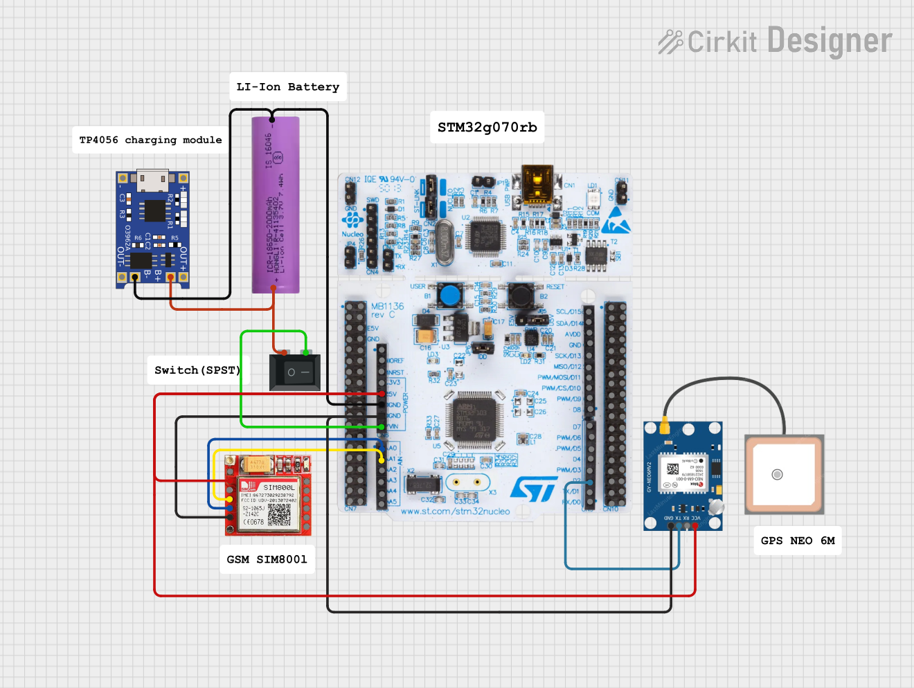 Open Project in Cirkit Designer
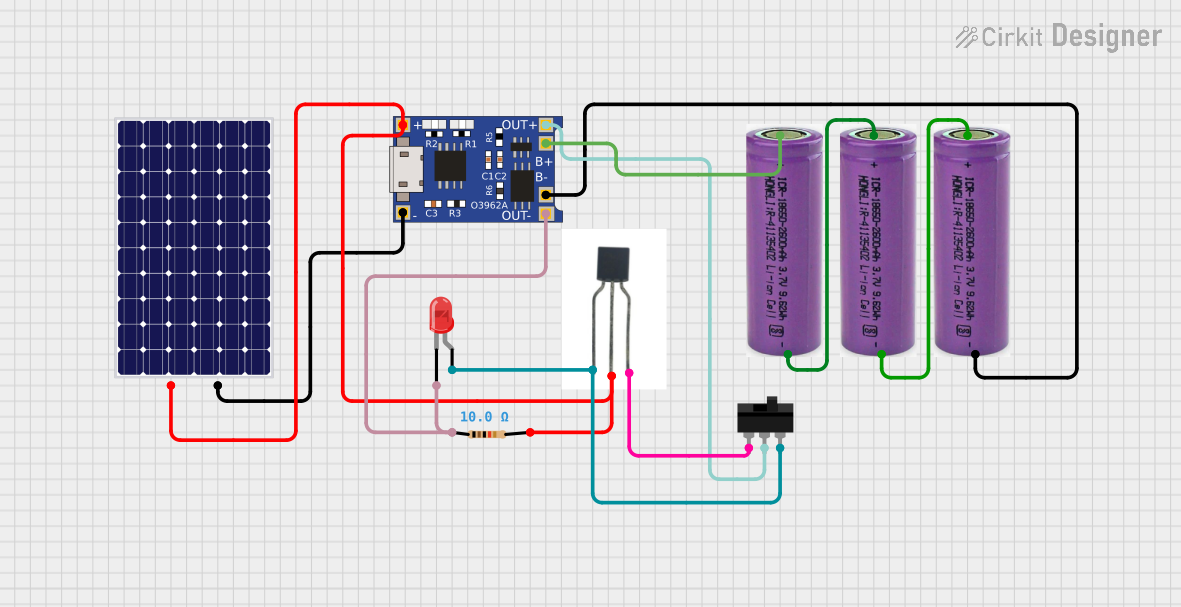 Open Project in Cirkit Designer
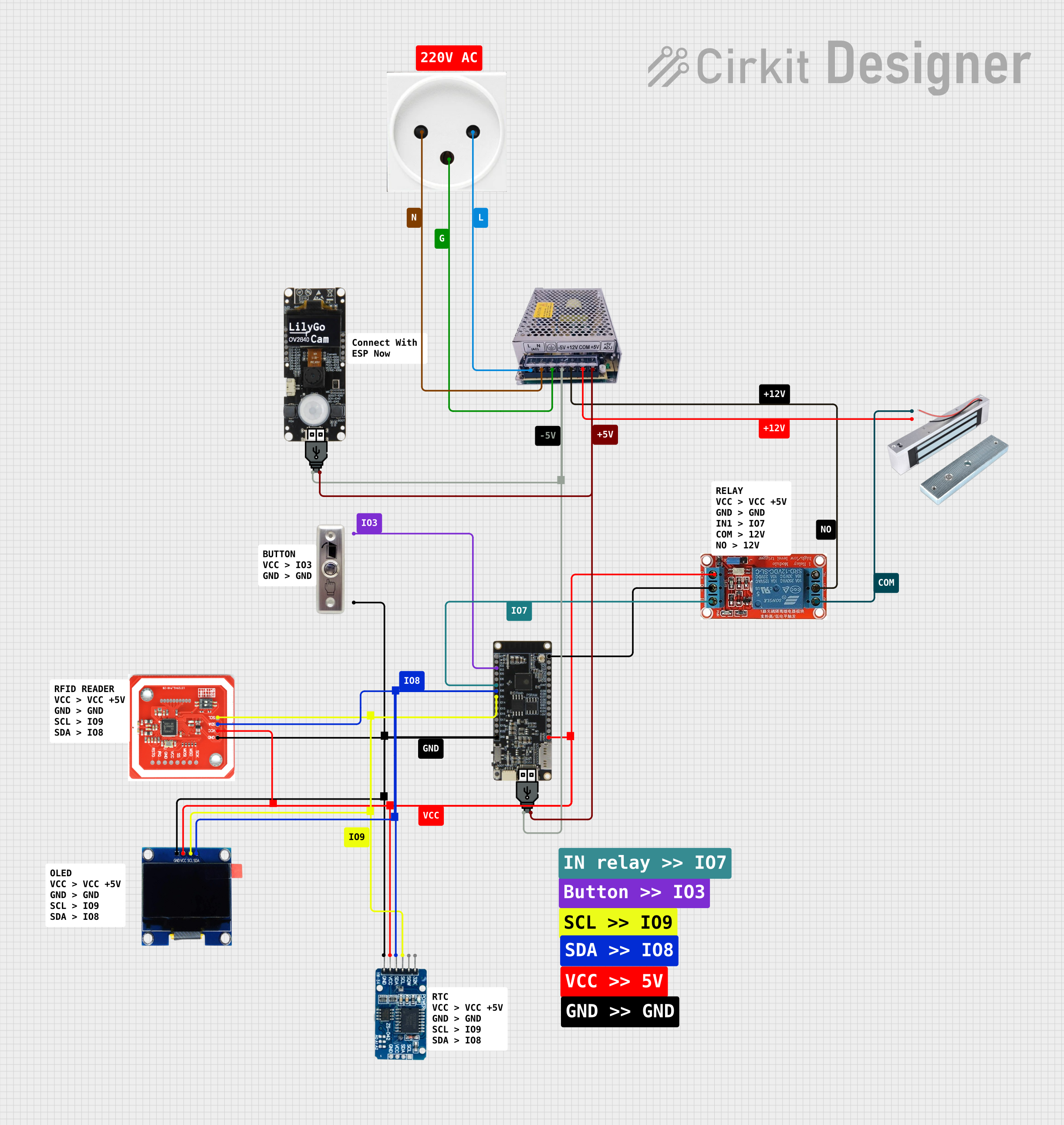 Open Project in Cirkit Designer
 Open Project in Cirkit Designer
Explore Projects Built with TS3A5017
Open Project in Cirkit DesignerOpen Project in Cirkit DesignerOpen Project in Cirkit DesignerOpen Project in Cirkit DesignerCommon Applications and Use Cases
- Audio signal switching in portable devices
- Video signal routing in multimedia systems
- Data communication switching in low-power systems
- General-purpose analog signal routing in embedded systems
- Multiplexing and demultiplexing in sensor networks
Technical Specifications
Key Technical Details
| Parameter | Value |
|---|---|
| Supply Voltage (Vcc) | 1.65 V to 3.6 V |
| On-Resistance (Ron) | 0.5 Ω (typical) |
| On-Resistance Flatness | 0.1 Ω (typical) |
| Bandwidth | 300 MHz |
| Supply Current (Icc) | 1 µA (maximum) |
| Operating Temperature Range | -40°C to +85°C |
| Package Type | SOIC-16 (TS3A5017DR) |
Pin Configuration and Descriptions
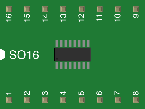
The TS3A5017 is available in a 16-pin SOIC package. Below is the pin configuration and description:
| Pin Number | Pin Name | Description |
|---|---|---|
| 1 | IN1 | Control input for switch 1 |
| 2 | COM1 | Common terminal for switch 1 |
| 3 | NO1 | Normally open terminal for switch 1 |
| 4 | NC1 | Normally closed terminal for switch 1 |
| 5 | GND | Ground |
| 6 | NC2 | Normally closed terminal for switch 2 |
| 7 | NO2 | Normally open terminal for switch 2 |
| 8 | COM2 | Common terminal for switch 2 |
| 9 | IN2 | Control input for switch 2 |
| 10 | V+ | Positive supply voltage |
| 11-16 | NC | No connection |
Usage Instructions
How to Use the TS3A5017 in a Circuit
- Power Supply: Connect the V+ pin to a supply voltage between 1.65 V and 3.6 V. Connect the GND pin to the ground of the circuit.
- Control Inputs: Use the IN1 and IN2 pins to control the state of the switches. A logic HIGH (V+) on the control pin connects the COM terminal to the NO terminal, while a logic LOW (GND) connects the COM terminal to the NC terminal.
- Signal Routing: Connect the signals you want to route to the NO, NC, and COM terminals of each switch. Ensure the signal levels are within the operating voltage range of the TS3A5017.
- Decoupling Capacitor: Place a 0.1 µF decoupling capacitor close to the V+ pin to stabilize the power supply.
Important Considerations and Best Practices
- Ensure the input signal levels do not exceed the supply voltage (V+).
- Minimize trace lengths to reduce parasitic capacitance and maintain signal integrity.
- Use pull-down resistors on the control pins (IN1, IN2) if they are left floating to avoid undefined states.
- For high-frequency signals, ensure proper PCB layout to minimize crosstalk and signal degradation.
Example: Connecting the TS3A5017 to an Arduino UNO
The TS3A5017 can be controlled using digital output pins from an Arduino UNO. Below is an example circuit and code to toggle the switches:
Circuit Connections
- Connect the V+ pin of the TS3A5017 to the 3.3V pin of the Arduino.
- Connect the GND pin of the TS3A5017 to the GND pin of the Arduino.
- Connect IN1 and IN2 to digital pins 7 and 8 of the Arduino, respectively.
- Connect the COM, NO, and NC terminals to the desired signal paths.
Arduino Code
// Define control pins for the TS3A5017
const int controlPin1 = 7; // Connected to IN1
const int controlPin2 = 8; // Connected to IN2

void setup() {
  // Set control pins as outputs
  pinMode(controlPin1, OUTPUT);
  pinMode(controlPin2, OUTPUT);

  // Initialize switches to default state (LOW)
  digitalWrite(controlPin1, LOW); // COM1 connected to NC1
  digitalWrite(controlPin2, LOW); // COM2 connected to NC2
}

void loop() {
  // Toggle switch 1
  digitalWrite(controlPin1, HIGH); // COM1 connected to NO1
  delay(1000); // Wait for 1 second
  digitalWrite(controlPin1, LOW);  // COM1 connected to NC1
  delay(1000); // Wait for 1 second

  // Toggle switch 2
  digitalWrite(controlPin2, HIGH); // COM2 connected to NO2
  delay(1000); // Wait for 1 second
  digitalWrite(controlPin2, LOW);  // COM2 connected to NC2
  delay(1000); // Wait for 1 second
}
Troubleshooting and FAQs
Common Issues and Solutions
Switch Not Responding to Control Signals
- Ensure the control pins (IN1, IN2) are properly connected to the microcontroller or control circuit.
- Verify that the control signal voltage levels match the supply voltage (V+).
Signal Distortion or Loss
- Check for excessive parasitic capacitance or long PCB traces.
- Ensure the input signal levels are within the specified range.
High Power Consumption
- Verify that the control pins are not left floating. Use pull-down resistors if necessary.
- Check for any short circuits or incorrect connections.
Unexpected Behavior
- Ensure the decoupling capacitor is properly placed near the V+ pin.
- Double-check the pin connections and verify the circuit design.
FAQs
Q1: Can the TS3A5017 handle digital signals?
A1: Yes, the TS3A5017 can handle both analog and digital signals as long as the signal levels are within the supply voltage range.
Q2: What is the maximum frequency the TS3A5017 can handle?
A2: The TS3A5017 has a bandwidth of 300 MHz, making it suitable for high-frequency applications.
Q3: Can I use the TS3A5017 with a 5V power supply?
A3: No, the TS3A5017 operates with a supply voltage range of 1.65 V to 3.6 V. Using a 5V supply may damage the component.
Q4: How do I reduce crosstalk between switches?
A4: Use proper PCB layout techniques, such as maintaining adequate spacing between traces and using ground planes to isolate signals.