
How to Use CA3140 BiMOS OP-AMP: Examples, Pinouts, and Specs
 Design with CA3140 BiMOS OP-AMP in Cirkit Designer
Introduction
The CA3140 BiMOS Operational Amplifier, manufactured by Renesas Electronics, is a high-performance op-amp that merges the benefits of bipolar and CMOS technologies. This hybrid design provides the CA3140 with exceptional characteristics such as low input bias current, high input impedance, and wide bandwidth. These features make it ideal for a wide range of analog applications, including signal processing, active filters, and precision amplifiers.
Explore Projects Built with CA3140 BiMOS OP-AMP
 Open Project in Cirkit Designer
 Open Project in Cirkit Designer
 Open Project in Cirkit Designer
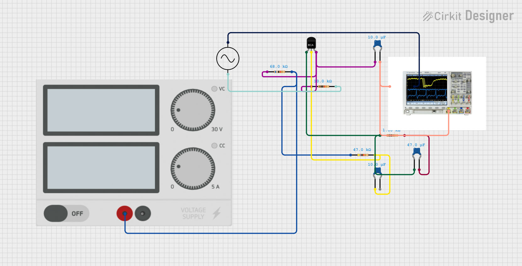 Open Project in Cirkit Designer
Explore Projects Built with CA3140 BiMOS OP-AMP
Open Project in Cirkit DesignerOpen Project in Cirkit DesignerOpen Project in Cirkit DesignerOpen Project in Cirkit DesignerCommon Applications
- Signal conditioning and processing
- Active filters and oscillators
- Voltage followers and buffers
- Analog computation circuits
- Medical instrumentation
- Data acquisition systems
Technical Specifications
Key Technical Details
| Parameter | Value |
|---|---|
| Supply Voltage (Vcc) | ±4V to ±18V (dual supply) or 8V to 36V (single supply) |
| Input Impedance | 1.5 TΩ (typical) |
| Input Bias Current | 10 pA (typical) |
| Gain Bandwidth Product | 4.5 MHz |
| Slew Rate | 9 V/µs |
| Output Voltage Swing | 0V to Vcc - 1.5V (single supply) |
| Operating Temperature Range | -55°C to +125°C |
| Package Types | DIP-8, SOIC-8 |
Pin Configuration and Descriptions
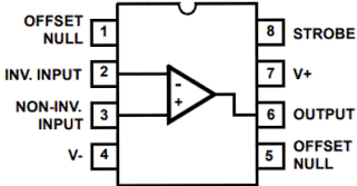
The CA3140 is typically available in an 8-pin DIP or SOIC package. Below is the pinout and description:
| Pin Number | Pin Name | Description |
|---|---|---|
| 1 | Offset Null 1 | Offset null adjustment (connect to a potentiometer) |
| 2 | Inverting Input | Inverting input terminal (-) |
| 3 | Non-Inverting Input | Non-inverting input terminal (+) |
| 4 | V- (GND) | Negative power supply or ground |
| 5 | Offset Null 2 | Offset null adjustment (connect to a potentiometer) |
| 6 | Output | Output terminal |
| 7 | V+ | Positive power supply |
| 8 | Strobe | Strobe pin (used to disable the output stage) |
Usage Instructions
How to Use the CA3140 in a Circuit
- Power Supply: Connect the op-amp to a suitable power supply. For single-supply operation, connect
V-(Pin 4) to ground andV+(Pin 7) to a positive voltage (e.g., 12V). For dual-supply operation, connectV-to a negative voltage (e.g., -12V) andV+to a positive voltage (e.g., +12V). - Input Connections: Connect the input signal to the inverting (
Pin 2) or non-inverting (Pin 3) terminal, depending on the desired configuration (e.g., inverting or non-inverting amplifier). - Output: The amplified signal will be available at the output terminal (
Pin 6). - Offset Nulling: If precise offset adjustment is required, connect a 10kΩ potentiometer between
Offset Null 1(Pin 1) andOffset Null 2(Pin 5), with the wiper connected toV+. - Strobe Pin: If not used, connect the strobe pin (
Pin 8) toV-to ensure normal operation.
Important Considerations and Best Practices
- Input Protection: Avoid applying input voltages that exceed the supply voltage range to prevent damage to the op-amp.
- Bypass Capacitors: Place decoupling capacitors (e.g., 0.1µF ceramic and 10µF electrolytic) close to the power supply pins to reduce noise and improve stability.
- Load Impedance: Ensure the load impedance is within the recommended range to avoid excessive current draw from the output.
- Strobe Function: Use the strobe pin to disable the output stage if needed, but ensure proper logic levels are applied.
Example: Connecting the CA3140 to an Arduino UNO
The CA3140 can be used with an Arduino UNO for signal amplification. Below is an example of using the CA3140 as a non-inverting amplifier:
Circuit Diagram
- Connect
V+(Pin 7) to the Arduino's 5V pin. - Connect
V-(Pin 4) to the Arduino's GND pin. - Connect the input signal to
Non-Inverting Input(Pin 3). - Connect a feedback resistor (e.g., 10kΩ) between
Output(Pin 6) andInverting Input(Pin 2). - Connect a resistor (e.g., 1kΩ) between
Inverting Input(Pin 2) and GND.
Arduino Code
// Example code for reading amplified signal from CA3140 using Arduino UNO

const int analogPin = A0; // Analog pin connected to CA3140 output
int signalValue = 0;      // Variable to store the analog signal value

void setup() {
  Serial.begin(9600); // Initialize serial communication at 9600 baud
}

void loop() {
  signalValue = analogRead(analogPin); // Read the amplified signal
  Serial.print("Amplified Signal Value: ");
  Serial.println(signalValue); // Print the signal value to the Serial Monitor
  delay(500); // Wait for 500ms before the next reading
}
Troubleshooting and FAQs
Common Issues and Solutions
No Output Signal:
- Ensure the power supply connections (
V+andV-) are correct and within the specified range. - Verify that the strobe pin (
Pin 8) is connected toV-if not in use. - Check for proper input signal connections.
- Ensure the power supply connections (
Distorted Output:
- Verify that the input signal amplitude is within the op-amp's input voltage range.
- Ensure the load impedance is not too low, as this can cause excessive current draw.
High Noise Levels:
- Add bypass capacitors near the power supply pins to reduce noise.
- Use shielded cables for input and output connections in noisy environments.
Offset Voltage Issues:
- Use a potentiometer connected to the offset null pins (
Pin 1andPin 5) to adjust the offset voltage.
- Use a potentiometer connected to the offset null pins (
FAQs
Q: Can the CA3140 operate with a single power supply?
A: Yes, the CA3140 can operate with a single supply voltage ranging from 8V to 36V. Connect V- to ground in this configuration.
Q: What is the purpose of the strobe pin?
A: The strobe pin allows the output stage to be disabled, effectively turning off the op-amp's output. If unused, connect it to V-.
Q: Is the CA3140 suitable for high-frequency applications?
A: The CA3140 has a gain bandwidth product of 4.5 MHz, making it suitable for moderate-frequency applications but not for very high-frequency designs.