How to Use CD4050BE: Examples, Pinouts, and Specs
Introduction
The CD4050BE is a hex buffer/driver IC designed to provide high input impedance and low output impedance. It is primarily used to strengthen weak logic signals, making it ideal for signal buffering and level shifting in digital circuits. This component is particularly useful in interfacing circuits where voltage level conversion is required, such as between 3.3V and 5V systems.
Explore Projects Built with CD4050BE
Explore Projects Built with CD4050BE
Common Applications and Use Cases
- Signal buffering to drive higher loads
- Voltage level shifting between different logic families
- Protecting sensitive components from high current or voltage
- Interfacing microcontrollers with other digital devices
- Driving LEDs or other low-power devices
Technical Specifications
The CD4050BE is a versatile IC with the following key specifications:
| Parameter | Value |
|---|---|
| Supply Voltage (Vcc) | 3V to 15V |
| Input Voltage Range | 0V to 15V |
| Output Voltage Range | 0V to Vcc |
| Maximum Output Current | ±3.4mA (at 5V Vcc) |
| Propagation Delay | ~60ns (at 5V Vcc) |
| Power Dissipation | 500mW |
| Operating Temperature | -55°C to +125°C |
| Package Type | DIP-16 (Dual Inline Package) |
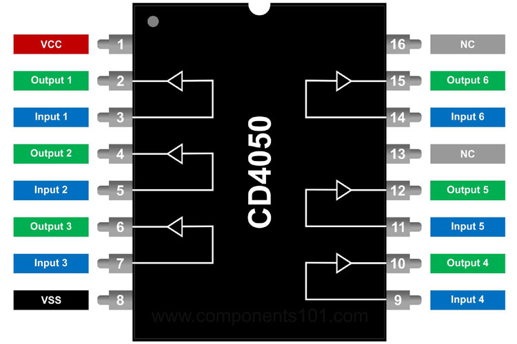
Pin Configuration and Descriptions
The CD4050BE has 16 pins, with six independent buffer channels. Below is the pinout and description:
| Pin Number | Pin Name | Description |
|---|---|---|
| 1 | NC | No Connection (not used) |
| 2 | A1 | Input for Buffer 1 |
| 3 | Y1 | Output for Buffer 1 |
| 4 | A2 | Input for Buffer 2 |
| 5 | Y2 | Output for Buffer 2 |
| 6 | A3 | Input for Buffer 3 |
| 7 | Y3 | Output for Buffer 3 |
| 8 | GND | Ground (0V reference) |
| 9 | Y4 | Output for Buffer 4 |
| 10 | A4 | Input for Buffer 4 |
| 11 | Y5 | Output for Buffer 5 |
| 12 | A5 | Input for Buffer 5 |
| 13 | Y6 | Output for Buffer 6 |
| 14 | A6 | Input for Buffer 6 |
| 15 | NC | No Connection (not used) |
| 16 | Vcc | Positive Supply Voltage |
Usage Instructions
How to Use the CD4050BE in a Circuit
- Power Supply: Connect the Vcc pin (Pin 16) to a voltage source within the range of 3V to 15V. Connect the GND pin (Pin 8) to the ground of the circuit.
- Input Signals: Apply the logic signals to the input pins (A1 to A6). Ensure the input voltage does not exceed the supply voltage (Vcc).
- Output Signals: The corresponding output pins (Y1 to Y6) will provide the buffered or level-shifted signals. These outputs can drive higher loads compared to the input signals.
- Unused Pins: Leave unused input pins floating or connect them to GND to avoid noise interference.
Important Considerations and Best Practices
- Voltage Compatibility: Ensure the input and output voltage levels are compatible with the devices being interfaced.
- Bypass Capacitor: Place a 0.1µF decoupling capacitor close to the Vcc pin to stabilize the power supply and reduce noise.
- Load Limitations: Do not exceed the maximum output current of ±3.4mA to avoid damaging the IC.
- Thermal Management: Operate the IC within the specified temperature range to ensure reliable performance.
Example: Using CD4050BE with Arduino UNO
The CD4050BE can be used to level-shift signals from a 5V Arduino UNO to a 3.3V device. Below is an example circuit and code:
Circuit Setup
- Connect the Arduino UNO's 5V pin to the CD4050BE's Vcc pin (Pin 16).
- Connect the Arduino UNO's GND pin to the CD4050BE's GND pin (Pin 8).
- Connect a 5V logic signal from the Arduino (e.g., Pin 7) to an input pin of the CD4050BE (e.g., A1, Pin 2).
- Connect the corresponding output pin (e.g., Y1, Pin 3) to the 3.3V device.
Arduino Code
// Example code to send a 5V signal from Arduino to a 3.3V device
const int outputPin = 7; // Arduino pin connected to CD4050BE input (A1)

void setup() {
  pinMode(outputPin, OUTPUT); // Set the pin as an output
}

void loop() {
  digitalWrite(outputPin, HIGH); // Send a HIGH signal (5V)
  delay(1000); // Wait for 1 second
  digitalWrite(outputPin, LOW); // Send a LOW signal (0V)
  delay(1000); // Wait for 1 second
}
Troubleshooting and FAQs
Common Issues and Solutions
No Output Signal:
- Ensure the IC is powered correctly (check Vcc and GND connections).
- Verify that the input signal is within the specified voltage range.
- Check for loose or incorrect wiring.
Output Voltage Too Low:
- Confirm that the load connected to the output does not exceed the maximum current rating.
- Use a bypass capacitor near the Vcc pin to reduce noise.
Overheating:
- Ensure the IC is not driving excessive current.
- Check for short circuits on the output pins.
Interference or Noise:
- Use proper grounding and shielding techniques.
- Add a decoupling capacitor to stabilize the power supply.
FAQs
Q: Can the CD4050BE be used for bidirectional level shifting?
A: No, the CD4050BE is designed for unidirectional signal buffering and level shifting. For bidirectional level shifting, consider using a dedicated level shifter IC.
Q: What happens if I leave input pins floating?
A: Floating input pins can pick up noise and cause erratic behavior. It is recommended to connect unused inputs to GND.
Q: Can I use the CD4050BE with a 3.3V power supply?
A: Yes, the CD4050BE can operate with a supply voltage as low as 3V. However, ensure that the input and output signals are compatible with the 3.3V logic level.
Q: Is the CD4050BE suitable for driving high-power devices?
A: No, the CD4050BE is not designed for high-power applications. Use a transistor or MOSFET driver for such cases.