How to Use Vendicta V2.5: Examples, Pinouts, and Specs
Introduction
The Vendicta V2.5 is a versatile and advanced circuit board designed for a wide range of applications. Manufactured by Vendicta, this component features enhanced processing capabilities, multiple input/output (I/O) options, and compatibility with various sensors and actuators. Its robust design and flexibility make it an excellent choice for robotics, automation, and IoT (Internet of Things) projects.
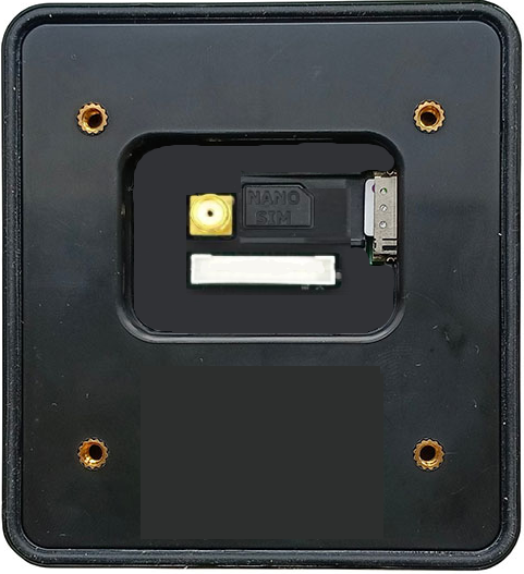
Explore Projects Built with Vendicta V2.5
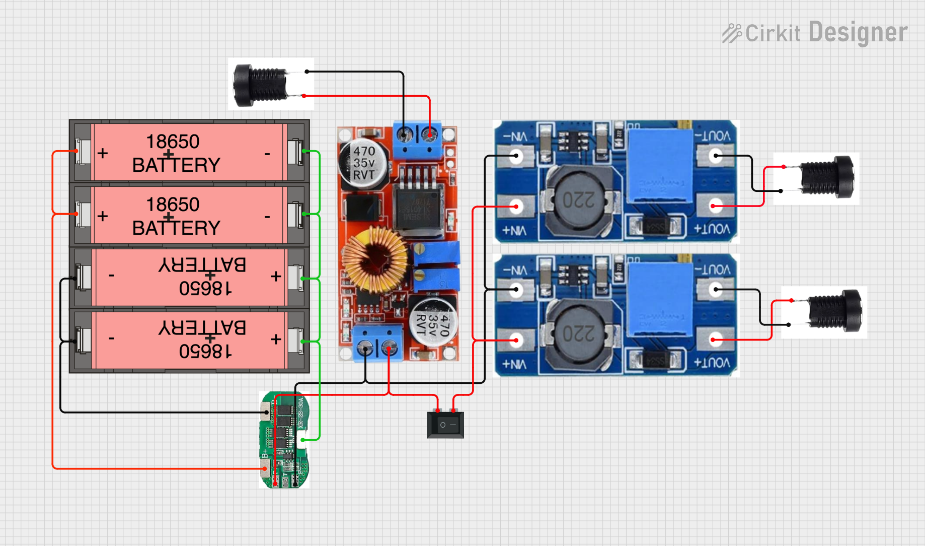
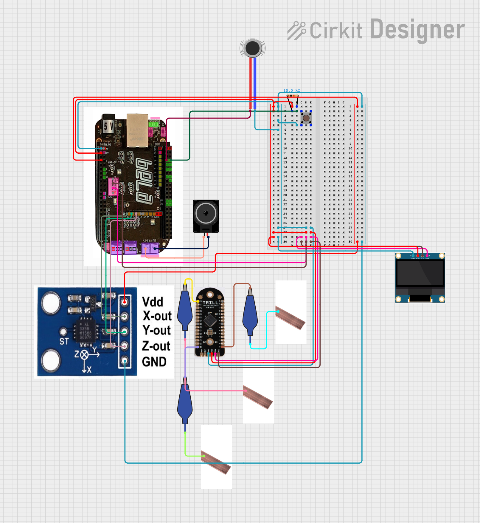
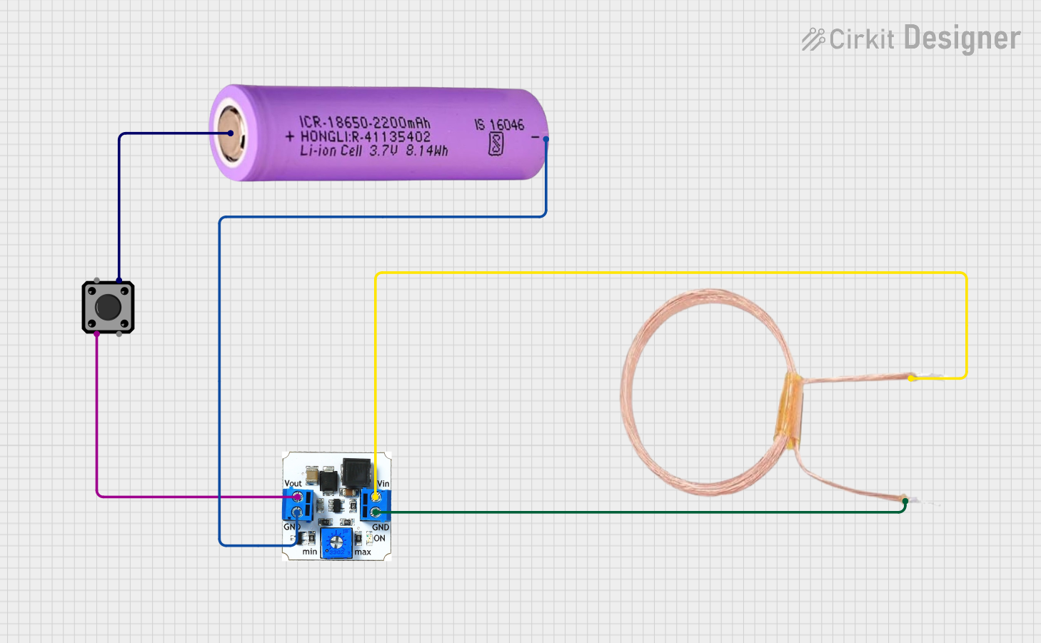
Explore Projects Built with Vendicta V2.5
Common Applications and Use Cases
- Robotics control systems
- Industrial automation
- IoT devices and smart home applications
- Sensor data acquisition and processing
- Actuator control for mechanical systems
- Educational and prototyping projects
Technical Specifications
The Vendicta V2.5 is engineered to deliver high performance and reliability. Below are its key technical specifications:
General Specifications
| Parameter | Value |
|---|---|
| Manufacturer | Vendicta |
| Model | V2.5 |
| Operating Voltage | 3.3V - 5V |
| Maximum Current | 1.5A |
| Processor | 32-bit ARM Cortex-M4 |
| Clock Speed | 120 MHz |
| Flash Memory | 512 KB |
| RAM | 128 KB |
| Communication Protocols | UART, I2C, SPI, CAN, USB |
| GPIO Pins | 20 |
| Analog Input Pins | 6 (10-bit resolution) |
| PWM Output Pins | 8 |
| Dimensions | 50mm x 50mm |
| Operating Temperature | -40°C to 85°C |
Pin Configuration and Descriptions
The Vendicta V2.5 features a 20-pin layout, with each pin serving a specific function. Below is the pin configuration:
| Pin Number | Pin Name | Description |
|---|---|---|
| 1 | VIN | Input voltage (3.3V - 5V) |
| 2 | GND | Ground |
| 3 | GPIO1 | General-purpose I/O pin |
| 4 | GPIO2 | General-purpose I/O pin |
| 5 | GPIO3 | General-purpose I/O pin |
| 6 | GPIO4 | General-purpose I/O pin |
| 7 | AIN1 | Analog input pin 1 |
| 8 | AIN2 | Analog input pin 2 |
| 9 | PWM1 | PWM output pin 1 |
| 10 | PWM2 | PWM output pin 2 |
| 11 | UART_TX | UART transmit pin |
| 12 | UART_RX | UART receive pin |
| 13 | I2C_SCL | I2C clock line |
| 14 | I2C_SDA | I2C data line |
| 15 | SPI_MOSI | SPI master-out, slave-in |
| 16 | SPI_MISO | SPI master-in, slave-out |
| 17 | SPI_SCK | SPI clock |
| 18 | CAN_H | CAN bus high line |
| 19 | CAN_L | CAN bus low line |
| 20 | USB_D+ | USB data positive |
Usage Instructions
The Vendicta V2.5 is designed for ease of use in a variety of circuits. Follow these steps and best practices to integrate it into your project:
Basic Setup
- Power Supply: Connect the VIN pin to a 3.3V or 5V power source and the GND pin to ground.
- I/O Connections: Use the GPIO pins for digital input/output, the AIN pins for analog input, and the PWM pins for controlling actuators like motors or LEDs.
- Communication: Utilize the UART, I2C, SPI, or CAN pins for communication with other devices or microcontrollers.
Example: Connecting to an Arduino UNO
The Vendicta V2.5 can be used as a peripheral device with an Arduino UNO. Below is an example of interfacing the Vendicta V2.5 via I2C:
Wiring
- Connect the
I2C_SCLpin of the Vendicta V2.5 to theA5pin of the Arduino UNO. - Connect the
I2C_SDApin of the Vendicta V2.5 to theA4pin of the Arduino UNO. - Connect the
VINpin of the Vendicta V2.5 to the5Vpin of the Arduino UNO. - Connect the
GNDpin of the Vendicta V2.5 to theGNDpin of the Arduino UNO.
Arduino Code
#include <Wire.h> // Include the Wire library for I2C communication

#define VENDICTA_I2C_ADDRESS 0x42 // Replace with the actual I2C address of Vendicta V2.5

void setup() {
  Wire.begin(); // Initialize I2C communication
  Serial.begin(9600); // Start serial communication for debugging
  Serial.println("Initializing Vendicta V2.5...");
}

void loop() {
  Wire.beginTransmission(VENDICTA_I2C_ADDRESS); // Start communication with Vendicta V2.5
  Wire.write(0x01); // Example: Send a command to the Vendicta V2.5
  Wire.endTransmission(); // End transmission

  delay(1000); // Wait for 1 second before repeating
}
Best Practices
- Use decoupling capacitors near the power pins to reduce noise.
- Avoid exceeding the maximum voltage and current ratings to prevent damage.
- Use proper pull-up resistors for I2C communication if not already integrated.
- Ensure proper grounding to avoid signal interference.
Troubleshooting and FAQs
Common Issues and Solutions
The Vendicta V2.5 does not power on.
- Ensure the VIN pin is connected to a stable 3.3V or 5V power source.
- Check for loose connections or damaged wires.
I2C communication is not working.
- Verify the I2C address of the Vendicta V2.5 and update the code accordingly.
- Check the pull-up resistors on the I2C lines.
Analog readings are inaccurate.
- Ensure the input voltage to the analog pins does not exceed the operating range.
- Use proper shielding to minimize noise interference.
PWM outputs are not functioning.
- Verify that the connected device (e.g., motor or LED) is compatible with the PWM signal.
- Check the duty cycle and frequency settings in your code.
FAQs
Q: Can the Vendicta V2.5 be used with 12V power supplies?
A: No, the Vendicta V2.5 operates within a voltage range of 3.3V to 5V. Using a 12V power supply may damage the board.
Q: Is the Vendicta V2.5 compatible with Raspberry Pi?
A: Yes, the Vendicta V2.5 can communicate with Raspberry Pi via UART, I2C, or SPI protocols.
Q: Does the Vendicta V2.5 support wireless communication?
A: The Vendicta V2.5 does not have built-in wireless capabilities, but you can connect external modules like Wi-Fi or Bluetooth via its communication pins.
Q: Can I use the Vendicta V2.5 in outdoor environments?
A: Yes, the Vendicta V2.5 is rated for an operating temperature range of -40°C to 85°C, making it suitable for outdoor use when properly enclosed.