How to Use 7476: Examples, Pinouts, and Specs
Introduction
The 7476 Dual J-K Flip-Flop, manufactured by HLF, is a versatile integrated circuit designed for storing binary data. It contains two independent J-K flip-flops, each equipped with J, K, clock, and asynchronous clear inputs. This component is widely used in digital electronics for applications such as counters, shift registers, and memory storage.
Explore Projects Built with 7476
Explore Projects Built with 7476
Common Applications
- Binary Counters: Used in sequential counting circuits.
- Frequency Division: Divides the frequency of an input clock signal.
- Data Storage: Stores binary data in digital systems.
- Shift Registers: Forms the building blocks of shift registers for data manipulation.
Technical Specifications
Key Technical Details
| Parameter | Value |
|---|---|
| Supply Voltage (Vcc) | 4.75V to 5.25V |
| Input Voltage (VI) | 0V to Vcc |
| High-Level Output (VOH) | 2.4V (min) |
| Low-Level Output (VOL) | 0.4V (max) |
| Propagation Delay | ~22ns (typical) |
| Power Dissipation | 25mW (typical) |
| Operating Temperature | 0°C to 70°C |
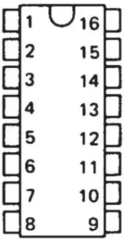
Pin Configuration and Descriptions
The 7476 IC is a 14-pin dual in-line package (DIP). Below is the pinout and description:
| Pin No. | Pin Name | Description |
|---|---|---|
| 1 | CLR1 | Asynchronous Clear Input for Flip-Flop 1 |
| 2 | CLK1 | Clock Input for Flip-Flop 1 |
| 3 | J1 | J Input for Flip-Flop 1 |
| 4 | K1 | K Input for Flip-Flop 1 |
| 5 | Q1 | Output Q for Flip-Flop 1 |
| 6 | Q1' | Complementary Output Q' for Flip-Flop 1 |
| 7 | GND | Ground |
| 8 | Q2' | Complementary Output Q' for Flip-Flop 2 |
| 9 | Q2 | Output Q for Flip-Flop 2 |
| 10 | K2 | K Input for Flip-Flop 2 |
| 11 | J2 | J Input for Flip-Flop 2 |
| 12 | CLK2 | Clock Input for Flip-Flop 2 |
| 13 | CLR2 | Asynchronous Clear Input for Flip-Flop 2 |
| 14 | Vcc | Positive Supply Voltage |
Usage Instructions
How to Use the 7476 in a Circuit
- Power Supply: Connect pin 14 to a +5V power supply and pin 7 to ground.
- Inputs: Provide the desired logic levels to the J and K inputs (pins 3, 4 for Flip-Flop 1 and pins 11, 10 for Flip-Flop 2).
- Clock Signal: Apply a clock signal to the CLK pins (pin 2 for Flip-Flop 1 and pin 12 for Flip-Flop 2). The flip-flop toggles its state on the rising edge of the clock.
- Clear Function: Use the CLR pins (pin 1 for Flip-Flop 1 and pin 13 for Flip-Flop 2) to asynchronously reset the outputs to 0, regardless of the clock state.
- Outputs: Monitor the Q and Q' outputs (pins 5, 6 for Flip-Flop 1 and pins 9, 8 for Flip-Flop 2) for the stored binary state.
Important Considerations
- Ensure the supply voltage does not exceed the specified range (4.75V to 5.25V).
- Avoid floating inputs; connect unused inputs to a defined logic level (e.g., ground or Vcc).
- Use decoupling capacitors (e.g., 0.1µF) near the IC to stabilize the power supply.
- The clock signal should have clean rising and falling edges to avoid erratic behavior.
Example: Connecting the 7476 to an Arduino UNO
The 7476 can be interfaced with an Arduino UNO to demonstrate its toggling behavior. Below is an example code snippet:
// Example: Toggling a 7476 Flip-Flop using Arduino UNO
// Connect CLK1 to Arduino pin 8, J1 to pin 9, K1 to pin 10, and CLR1 to pin 11.

#define CLK1 8  // Clock input for Flip-Flop 1
#define J1 9    // J input for Flip-Flop 1
#define K1 10   // K input for Flip-Flop 1
#define CLR1 11 // Clear input for Flip-Flop 1

void setup() {
  pinMode(CLK1, OUTPUT); // Set CLK1 as output
  pinMode(J1, OUTPUT);   // Set J1 as output
  pinMode(K1, OUTPUT);   // Set K1 as output
  pinMode(CLR1, OUTPUT); // Set CLR1 as output

  digitalWrite(CLR1, HIGH); // Ensure CLR1 is inactive (logic HIGH)
  digitalWrite(J1, HIGH);   // Set J1 to logic HIGH
  digitalWrite(K1, HIGH);   // Set K1 to logic HIGH
}

void loop() {
  digitalWrite(CLK1, HIGH); // Generate a clock pulse
  delay(100);               // Wait for 100ms
  digitalWrite(CLK1, LOW);  // End the clock pulse
  delay(100);               // Wait for 100ms
}
Explanation of the Code
- The J1 and K1 inputs are set to HIGH, enabling the toggle mode of the flip-flop.
- A clock pulse is generated on CLK1 every 100ms, causing the flip-flop to toggle its state.
- The CLR1 input is kept HIGH to ensure the flip-flop is not asynchronously cleared.
Troubleshooting and FAQs
Common Issues and Solutions
No Output on Q or Q' Pins:
- Ensure the power supply is connected correctly (pin 14 to +5V, pin 7 to GND).
- Verify that the clock signal is being applied to the CLK pin.
- Check that the J and K inputs are not left floating.
Erratic Behavior:
- Use a clean clock signal with sharp rising and falling edges.
- Add decoupling capacitors near the IC to reduce noise.
Outputs Not Toggling:
- Confirm that both J and K inputs are HIGH for toggle mode.
- Check the connections to the clock input and ensure it is receiving pulses.
FAQs
Q1: Can the 7476 operate at voltages other than 5V?
A1: No, the 7476 is designed to operate within a supply voltage range of 4.75V to 5.25V. Operating outside this range may damage the IC.
Q2: What happens if the CLR pin is activated?
A2: Activating the CLR pin (logic LOW) asynchronously resets the Q output to 0 and Q' to 1, regardless of the clock or J/K inputs.
Q3: Can I use the 7476 for edge-triggered applications?
A3: Yes, the 7476 is edge-triggered and responds to the rising edge of the clock signal.
Q4: How do I prevent unused flip-flops from interfering with my circuit?
A4: Tie the unused J and K inputs to ground and leave the corresponding clock and clear inputs unconnected.