
How to Use SN74LVC2G14DBVR: Examples, Pinouts, and Specs
 Design with SN74LVC2G14DBVR in Cirkit Designer
Introduction
The SN74LVC2G14DBVR is a dual Schmitt-trigger inverter manufactured by Texas Instruments. This component is designed to operate with a supply voltage range of 1.65V to 5.5V, making it suitable for a wide variety of digital logic applications. Its Schmitt-trigger inputs provide high noise immunity and fast switching speeds, ensuring reliable performance in noisy environments or when dealing with slow input signal transitions.
Explore Projects Built with SN74LVC2G14DBVR
 Open Project in Cirkit Designer
 Open Project in Cirkit Designer
 Open Project in Cirkit Designer
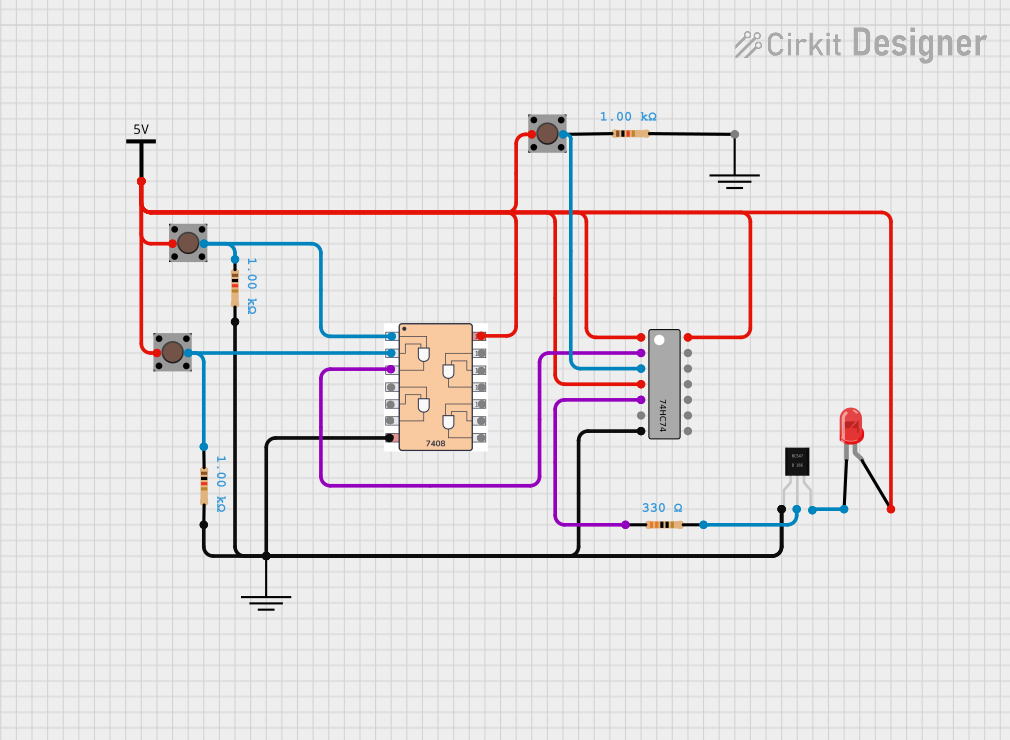 Open Project in Cirkit Designer
Explore Projects Built with SN74LVC2G14DBVR
Open Project in Cirkit DesignerOpen Project in Cirkit DesignerOpen Project in Cirkit DesignerOpen Project in Cirkit DesignerCommon Applications
- Signal conditioning and waveform shaping
- Noise filtering in digital circuits
- Logic level conversion
- Clock and data signal inversion
- Use in microcontroller-based systems for input/output signal processing
Technical Specifications
Key Technical Details
| Parameter | Value |
|---|---|
| Supply Voltage (Vcc) | 1.65V to 5.5V |
| Input Voltage Range (VI) | 0V to 5.5V |
| Output Voltage Range (VO) | 0V to Vcc |
| High-Level Output Current | -32mA |
| Low-Level Output Current | 32mA |
| Input Threshold Voltage | Varies with Vcc (Schmitt-trigger input) |
| Propagation Delay (tpd) | 3.8ns (typical at 3.3V) |
| Operating Temperature Range | -40°C to 125°C |
| Package Type | SOT-23-6 (DBV) |
Pin Configuration and Descriptions
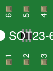
The SN74LVC2G14DBVR is housed in a 6-pin SOT-23 package. The pinout and descriptions are as follows:
| Pin Number | Pin Name | Description |
|---|---|---|
| 1 | 1A | Input to the first inverter |
| 2 | 1Y | Output of the first inverter |
| 3 | GND | Ground (0V reference) |
| 4 | 2A | Input to the second inverter |
| 5 | 2Y | Output of the second inverter |
| 6 | Vcc | Positive supply voltage |
Usage Instructions
How to Use the Component in a Circuit
- Power Supply: Connect the Vcc pin (Pin 6) to a stable power supply within the range of 1.65V to 5.5V. Connect the GND pin (Pin 3) to the ground of the circuit.
- Input Signals: Apply the input signals to the 1A (Pin 1) and 2A (Pin 4) pins. Ensure that the input voltage levels are within the specified range (0V to 5.5V).
- Output Signals: The inverted outputs will be available at 1Y (Pin 2) and 2Y (Pin 5). These outputs will switch based on the Schmitt-trigger characteristics, providing clean transitions even with noisy or slow input signals.
- Bypass Capacitor: Place a decoupling capacitor (e.g., 0.1µF) close to the Vcc pin to filter out power supply noise.
Important Considerations and Best Practices
- Input Signal Characteristics: The Schmitt-trigger inputs are designed to handle slow or noisy signals. Ensure that the input signals do not exceed the maximum input voltage rating of 5.5V.
- Unused Inputs: Tie any unused inputs (1A or 2A) to GND or Vcc to prevent floating inputs, which can cause unpredictable behavior.
- Output Loading: Avoid exceeding the maximum output current rating of ±32mA to prevent damage to the device.
- PCB Layout: Minimize trace lengths for the input and output signals to reduce noise and signal degradation.
Example: Connecting to an Arduino UNO
The SN74LVC2G14DBVR can be used with an Arduino UNO to invert a digital signal. Below is an example circuit and code:
Circuit
- Connect the Vcc pin (Pin 6) to the Arduino's 5V pin.
- Connect the GND pin (Pin 3) to the Arduino's GND pin.
- Connect an Arduino digital output pin (e.g., D2) to the 1A pin (Pin 1).
- Connect the 1Y pin (Pin 2) to an LED (with a current-limiting resistor) or another circuit.
Code
// Arduino code to demonstrate signal inversion using SN74LVC2G14DBVR

void setup() {
  pinMode(2, OUTPUT); // Set pin 2 as an output
  pinMode(3, INPUT);  // Set pin 3 as an input (connected to 1Y output)
}

void loop() {
  digitalWrite(2, HIGH); // Send a HIGH signal to the inverter input
  delay(1000);           // Wait for 1 second
  digitalWrite(2, LOW);  // Send a LOW signal to the inverter input
  delay(1000);           // Wait for 1 second
}
Troubleshooting and FAQs
Common Issues and Solutions
No Output Signal:
- Ensure that the Vcc and GND pins are properly connected.
- Verify that the input signal is within the specified voltage range.
- Check for loose or incorrect connections in the circuit.
Unstable or Noisy Output:
- Add a decoupling capacitor (e.g., 0.1µF) near the Vcc pin to stabilize the power supply.
- Ensure that the input signal is not floating. Tie unused inputs to GND or Vcc.
Component Overheating:
- Verify that the output current does not exceed the maximum rating of ±32mA.
- Check for short circuits or excessive loading on the output pins.
FAQs
Q1: Can the SN74LVC2G14DBVR operate at 3.3V?
A1: Yes, the component operates reliably within a supply voltage range of 1.65V to 5.5V, including 3.3V.
Q2: What is the advantage of Schmitt-trigger inputs?
A2: Schmitt-trigger inputs provide hysteresis, which improves noise immunity and ensures clean signal transitions even with slow or noisy input signals.
Q3: Can I use this component for level shifting?
A3: Yes, the SN74LVC2G14DBVR can be used for level shifting within its specified voltage range, as long as the input and output levels are compatible with the connected devices.
Q4: What happens if I leave an input pin floating?
A4: Floating input pins can cause unpredictable behavior. Always tie unused inputs to GND or Vcc.