
How to Use HCF4067B 16-channel analog multiplexer (DIP-24): Examples, Pinouts, and Specs
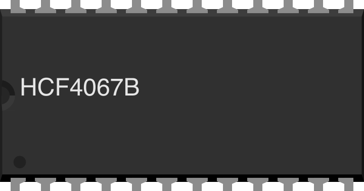
 Design with HCF4067B 16-channel analog multiplexer (DIP-24) in Cirkit Designer
Introduction
The HCF4067B, manufactured by STMicroelectronics, is a versatile 16-channel analog multiplexer/demultiplexer. It allows the selection of one of 16 input signals to be routed to a single output, or vice versa. This component supports both analog and digital signals, making it ideal for signal routing, data acquisition systems, and sensor multiplexing.
Explore Projects Built with HCF4067B 16-channel analog multiplexer (DIP-24)
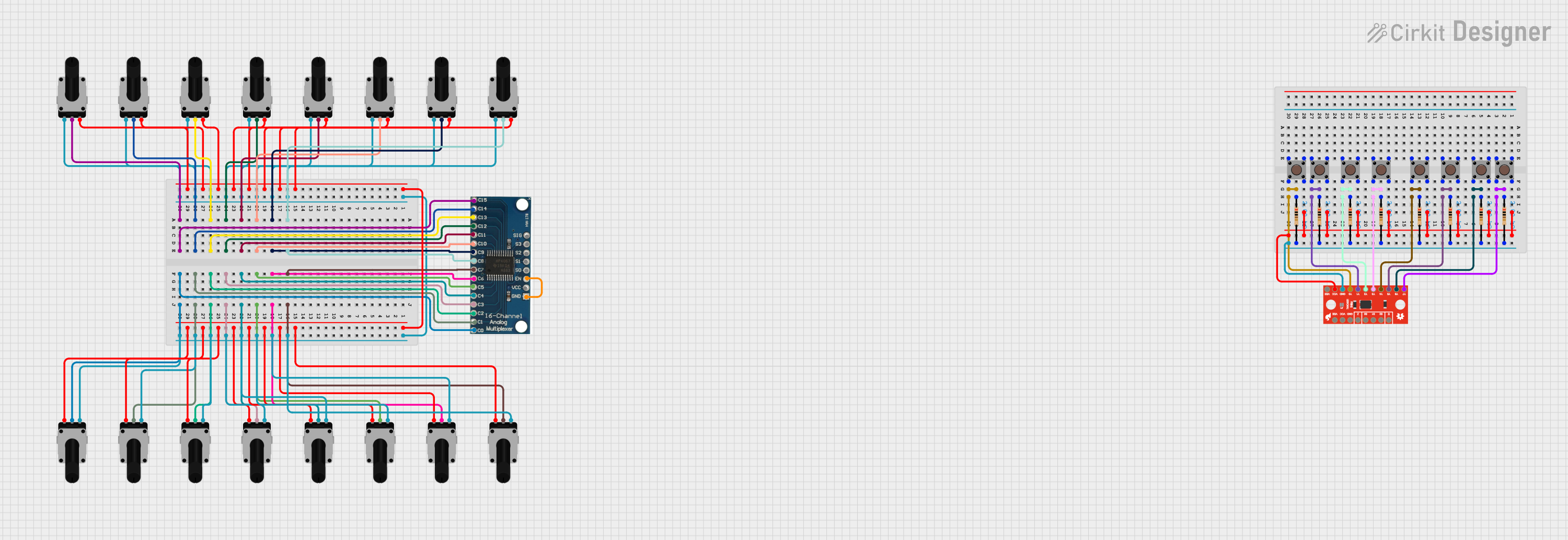 Open Project in Cirkit Designer
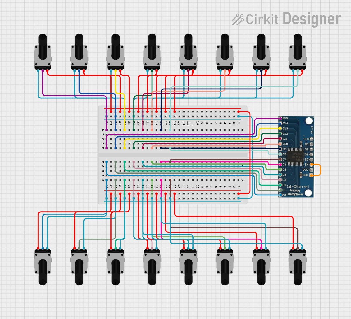 Open Project in Cirkit Designer
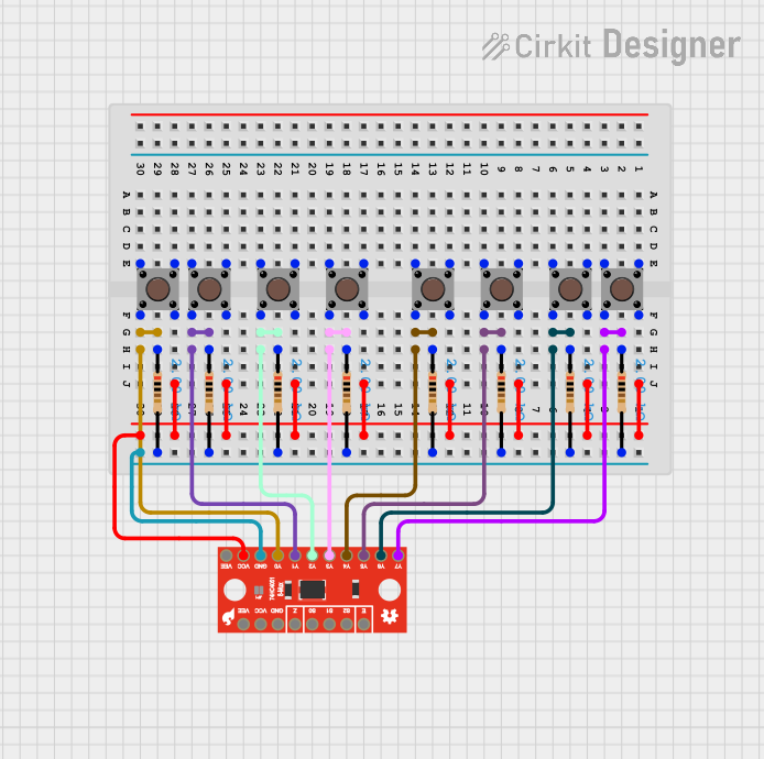 Open Project in Cirkit Designer
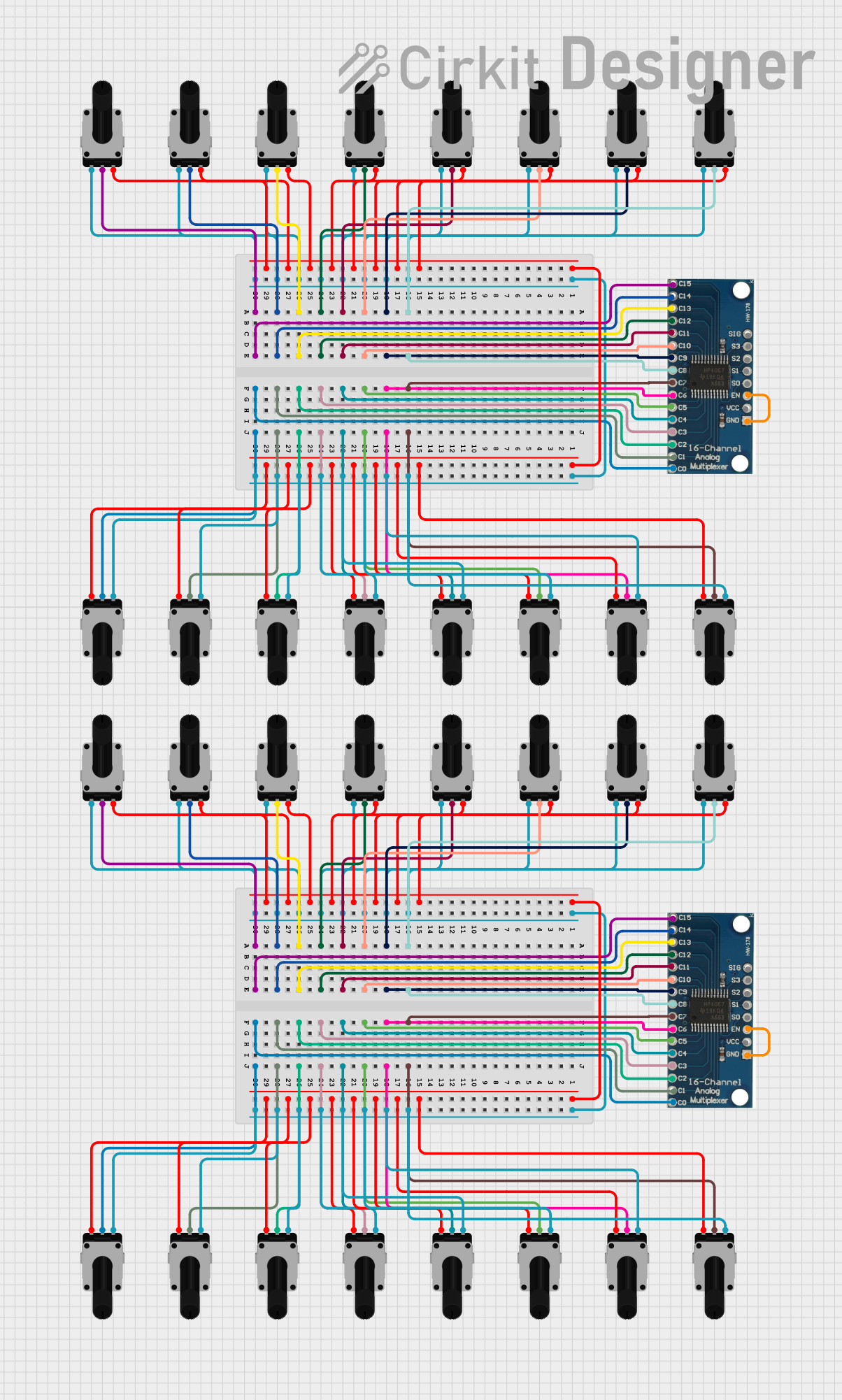 Open Project in Cirkit Designer
Explore Projects Built with HCF4067B 16-channel analog multiplexer (DIP-24)
Open Project in Cirkit DesignerOpen Project in Cirkit DesignerOpen Project in Cirkit DesignerOpen Project in Cirkit DesignerCommon Applications and Use Cases
- Signal routing in data acquisition systems
- Sensor multiplexing in embedded systems
- Audio signal switching
- Expanding the number of analog inputs for microcontrollers
- Digital signal selection in logic circuits
Technical Specifications
The HCF4067B is designed for high-performance signal switching and routing. Below are its key technical details:
Key Technical Details
- Operating Voltage (VDD): 3V to 15V
- Input Signal Range: 0V to VDD
- On-Resistance (RON): 70Ω (typical at VDD = 10V)
- Maximum Input Current: ±10mA
- Propagation Delay: 50ns (typical at VDD = 10V)
- Power Dissipation: 700mW (maximum)
- Package Type: DIP-24
- Temperature Range: -55°C to +125°C
Pin Configuration and Descriptions
The HCF4067B is housed in a 24-pin DIP package. Below is the pinout and description:
| Pin Number | Pin Name | Description |
|---|---|---|
| 1 | S0 | Address select input (Least Significant Bit - LSB) |
| 2 | S1 | Address select input |
| 3 | S2 | Address select input |
| 4 | S3 | Address select input (Most Significant Bit - MSB) |
| 5 | Z | Common output/input (multiplexer/demultiplexer shared terminal) |
| 6-21 | Y0-Y15 | Channel inputs/outputs (Y0 to Y15) |
| 22 | INH | Inhibit control (active HIGH, disables all channels when HIGH) |
| 23 | VSS | Ground (0V reference) |
| 24 | VDD | Positive supply voltage |
Usage Instructions
The HCF4067B is straightforward to use in both analog and digital circuits. Below are the steps and considerations for integrating it into your design.
How to Use the Component in a Circuit
Power Supply:
- Connect the VDD pin to the positive supply voltage (3V to 15V).
- Connect the VSS pin to ground (0V).
Address Selection:
- Use the S0-S3 pins to select one of the 16 channels. The binary value on these pins determines the active channel:
- Example:
S3 S2 S1 S0 = 0000selects channel Y0, and1111selects channel Y15.
- Example:
- Use the S0-S3 pins to select one of the 16 channels. The binary value on these pins determines the active channel:
Signal Routing:
- Connect the signal sources to the Y0-Y15 pins.
- The selected channel will route its signal to the Z pin (or vice versa for demultiplexing).
Inhibit Control:
- When the INH pin is HIGH, all channels are disabled, and no signal is routed to/from the Z pin.
Analog Signal Handling:
- Ensure the input signal voltage stays within the range of 0V to VDD to avoid damage.
Important Considerations and Best Practices
- Decoupling Capacitor: Place a 0.1µF ceramic capacitor close to the VDD pin to stabilize the power supply.
- Signal Integrity: For high-frequency signals, minimize trace lengths to reduce noise and signal degradation.
- Unused Inputs: Tie unused address pins (S0-S3) to ground or VDD to avoid floating inputs.
- Voltage Compatibility: Ensure the control signals (S0-S3, INH) are compatible with the VDD voltage level.
Example: Connecting to an Arduino UNO
The HCF4067B can be easily interfaced with an Arduino UNO for channel selection. Below is an example code snippet:
// Define address pins connected to Arduino
const int S0 = 2;  // Connect S0 to Arduino pin 2
const int S1 = 3;  // Connect S1 to Arduino pin 3
const int S2 = 4;  // Connect S2 to Arduino pin 4
const int S3 = 5;  // Connect S3 to Arduino pin 5

// Define the common I/O pin
const int Z = A0;  // Connect Z to Arduino analog pin A0

void setup() {
  // Set address pins as outputs
  pinMode(S0, OUTPUT);
  pinMode(S1, OUTPUT);
  pinMode(S2, OUTPUT);
  pinMode(S3, OUTPUT);

  // Initialize serial communication for debugging
  Serial.begin(9600);
}

void loop() {
  for (int channel = 0; channel < 16; channel++) {
    // Set the address pins to select the channel
    digitalWrite(S0, channel & 0x01);  // LSB
    digitalWrite(S1, (channel >> 1) & 0x01);
    digitalWrite(S2, (channel >> 2) & 0x01);
    digitalWrite(S3, (channel >> 3) & 0x01);

    // Read the signal from the selected channel
    int signal = analogRead(Z);

    // Print the channel and signal value
    Serial.print("Channel ");
    Serial.print(channel);
    Serial.print(": ");
    Serial.println(signal);

    delay(500);  // Wait for 500ms before switching to the next channel
  }
}
Troubleshooting and FAQs
Common Issues and Solutions
No Signal on Output (Z):
- Ensure the INH pin is LOW. If HIGH, all channels are disabled.
- Verify the address pins (S0-S3) are set correctly for the desired channel.
Signal Distortion:
- Check if the input signal voltage exceeds the range of 0V to VDD.
- Minimize trace lengths and use proper shielding for high-frequency signals.
High On-Resistance:
- The on-resistance increases at lower supply voltages. Use a higher VDD (within the specified range) for better performance.
Floating Inputs:
- Tie unused address pins (S0-S3) to a defined logic level (HIGH or LOW) to avoid erratic behavior.
FAQs
Q: Can the HCF4067B handle bi-directional signals?
A: Yes, the HCF4067B supports bi-directional signal routing, making it suitable for both multiplexing and demultiplexing.
Q: What is the maximum frequency the HCF4067B can handle?
A: The maximum frequency depends on the supply voltage and load conditions. For typical applications, it can handle signals up to a few MHz.
Q: Can I use the HCF4067B with 5V logic systems?
A: Yes, the HCF4067B is compatible with 5V logic systems when VDD is set to 5V.
Q: How do I disable all channels?
A: Set the INH pin HIGH to disable all channels and disconnect the Z pin from any input/output.