
How to Use SO-24W: Examples, Pinouts, and Specs
 Design with SO-24W in Cirkit Designer
Introduction
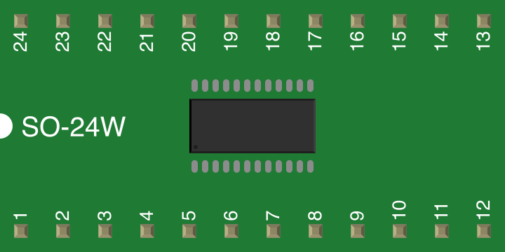
The SO-24W (Small Outline 24-Wide) is a surface-mount integrated circuit (IC) package featuring 24 pins. It is designed for compact and efficient integration into printed circuit boards (PCBs). The wide-body design provides additional spacing between pins, making it suitable for applications requiring enhanced electrical isolation or higher power handling. Its small form factor and reliability make it a popular choice in modern electronics.
Explore Projects Built with SO-24W
 Open Project in Cirkit Designer
 Open Project in Cirkit Designer
 Open Project in Cirkit Designer
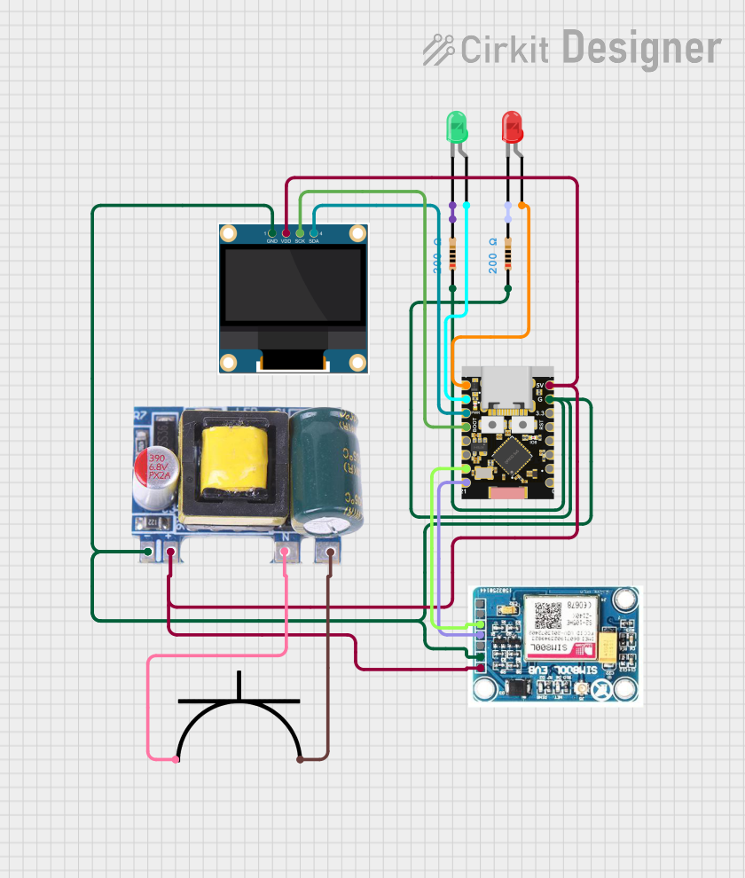 Open Project in Cirkit Designer
Explore Projects Built with SO-24W
Open Project in Cirkit DesignerOpen Project in Cirkit DesignerOpen Project in Cirkit DesignerOpen Project in Cirkit DesignerCommon Applications and Use Cases
- Microcontrollers and digital ICs
- Analog-to-digital converters (ADCs) and digital-to-analog converters (DACs)
- Power management ICs
- Communication modules
- Signal processing circuits
- Consumer electronics, automotive systems, and industrial equipment
Technical Specifications
The SO-24W package is designed to meet the needs of a wide range of electronic applications. Below are its key technical details:
Key Specifications
| Parameter | Value |
|---|---|
| Number of Pins | 24 |
| Package Type | Small Outline (Wide Body) |
| Pin Pitch | 1.27 mm |
| Body Width | 7.5 mm |
| Body Length | 15.4 mm |
| Maximum Height | 2.65 mm |
| Thermal Resistance (θJA) | Typically 80–120 °C/W |
| Mounting Type | Surface Mount |
| Operating Temperature | -40 °C to +125 °C (varies by IC) |
| Lead Finish | Matte Tin or Lead-Free Options |
Pin Configuration and Descriptions
The SO-24W package has 24 pins arranged in two parallel rows. The pin configuration depends on the specific IC housed in the package. Below is a generic example of pin descriptions for a microcontroller IC in an SO-24W package:
| Pin Number | Pin Name | Description |
|---|---|---|
| 1 | VCC | Power supply input |
| 2 | GND | Ground |
| 3 | RESET | Reset input |
| 4 | GPIO1 | General-purpose input/output pin 1 |
| 5 | GPIO2 | General-purpose input/output pin 2 |
| 6 | TXD | UART Transmit |
| 7 | RXD | UART Receive |
| 8 | PWM1 | Pulse-width modulation output 1 |
| 9 | PWM2 | Pulse-width modulation output 2 |
| 10 | ADC_IN1 | Analog-to-digital converter input 1 |
| 11 | ADC_IN2 | Analog-to-digital converter input 2 |
| 12 | SPI_MOSI | SPI Master Out Slave In |
| 13 | SPI_MISO | SPI Master In Slave Out |
| 14 | SPI_SCK | SPI Clock |
| 15 | SPI_CS | SPI Chip Select |
| 16 | I2C_SDA | I2C Data Line |
| 17 | I2C_SCL | I2C Clock Line |
| 18 | GPIO3 | General-purpose input/output pin 3 |
| 19 | GPIO4 | General-purpose input/output pin 4 |
| 20 | INT1 | External interrupt input 1 |
| 21 | INT2 | External interrupt input 2 |
| 22 | VREF | Voltage reference input |
| 23 | OSC_IN | Oscillator input |
| 24 | OSC_OUT | Oscillator output |
Note: The actual pin configuration may vary depending on the IC housed in the SO-24W package. Always refer to the specific IC datasheet for accurate pin descriptions.
Usage Instructions
How to Use the SO-24W in a Circuit
- PCB Design: Ensure the PCB layout matches the SO-24W footprint. The pin pitch is 1.27 mm, and the wide-body design requires a body width of 7.5 mm.
- Soldering: Use surface-mount soldering techniques such as reflow soldering. Ensure proper alignment of the pins with the PCB pads.
- Power Supply: Verify the voltage and current requirements of the IC housed in the SO-24W package. Connect the VCC and GND pins appropriately.
- Signal Connections: Connect the input/output pins (e.g., GPIO, UART, SPI, I2C) to the corresponding components in your circuit.
- Bypass Capacitors: Place decoupling capacitors (e.g., 0.1 µF) near the VCC pin to reduce noise and stabilize the power supply.
Important Considerations and Best Practices
- Thermal Management: Ensure adequate heat dissipation, especially for high-power ICs. Use thermal vias or heat sinks if necessary.
- Signal Integrity: Minimize trace lengths for high-speed signals to reduce noise and signal degradation.
- ESD Protection: Handle the SO-24W package with care to prevent electrostatic discharge (ESD) damage.
- IC-Specific Requirements: Always consult the datasheet of the specific IC housed in the SO-24W package for detailed usage instructions.
Example: Connecting an SO-24W Microcontroller to an Arduino UNO
If the SO-24W package contains a microcontroller, you can interface it with an Arduino UNO using UART communication. Below is an example Arduino sketch:
// Example: Communicating with an SO-24W microcontroller via UART
// Connect SO-24W TXD to Arduino RX (Pin 0)
// Connect SO-24W RXD to Arduino TX (Pin 1)
// Ensure a common ground connection between the Arduino and SO-24W

void setup() {
  Serial.begin(9600); // Initialize UART communication at 9600 baud
  Serial.println("Arduino is ready to communicate with SO-24W!");
}

void loop() {
  // Check if data is available from the SO-24W microcontroller
  if (Serial.available() > 0) {
    String data = Serial.readString(); // Read incoming data
    Serial.print("Received: ");
    Serial.println(data); // Print the received data
  }

  // Send data to the SO-24W microcontroller
  Serial.println("Hello from Arduino!");
  delay(1000); // Wait for 1 second before sending the next message
}
Note: Ensure the voltage levels of the SO-24W microcontroller and Arduino UNO are compatible. Use a level shifter if necessary.
Troubleshooting and FAQs
Common Issues
Misaligned Pins During Soldering
- Cause: Improper placement of the SO-24W package on the PCB.
- Solution: Use a stencil and reflow soldering process for precise alignment.
Overheating
- Cause: Insufficient thermal management.
- Solution: Add thermal vias or heat sinks to dissipate heat effectively.
Communication Errors
- Cause: Incorrect connections or mismatched voltage levels.
- Solution: Verify pin connections and use level shifters if required.
No Output Signal
- Cause: Missing or incorrect power supply.
- Solution: Check the VCC and GND connections and ensure the correct voltage is supplied.
FAQs
Q1: Can the SO-24W package be hand-soldered?
A1: Yes, but it requires precision and a fine-tipped soldering iron. Reflow soldering is recommended for better results.
Q2: What is the difference between SO-24 and SO-24W?
A2: The SO-24W has a wider body (7.5 mm) compared to the standard SO-24 (5.3 mm), providing better electrical isolation and thermal performance.
Q3: How do I identify pin 1 on the SO-24W package?
A3: Pin 1 is typically marked with a dot or notch on the package. Refer to the IC datasheet for exact details.
Q4: Can I use the SO-24W package for high-frequency applications?
A4: Yes, but ensure proper PCB design practices, such as minimizing trace lengths and using ground planes, to maintain signal integrity.