How to Use 74x76: Examples, Pinouts, and Specs
Introduction
The 74x76 is a type of integrated circuit (IC) that belongs to the 7400 series of logic chips, manufactured by Motorola under the part ID dsadas. This IC is commonly used for implementing various logic functions in digital circuits. Specifically, the 74x76 is a dual J-K flip-flop with preset and clear inputs, making it ideal for applications requiring bistable multivibrators, data storage, or frequency division.
Explore Projects Built with 74x76
Explore Projects Built with 74x76
Common Applications and Use Cases
- Data Storage: Used in digital systems to store binary data.
- Frequency Division: Acts as a frequency divider in clock circuits.
- State Machines: Forms the building blocks of sequential logic circuits.
- Counters and Registers: Used in counters, shift registers, and other sequential circuits.
Technical Specifications
Key Technical Details
- Logic Family: 7400 series
- Function: Dual J-K flip-flop with preset and clear
- Supply Voltage (Vcc): 4.75V to 5.25V (typical 5V)
- Input Voltage (VIH): Minimum 2V for logic HIGH
- Input Voltage (VIL): Maximum 0.8V for logic LOW
- Output Voltage (VOH): Minimum 2.4V for logic HIGH
- Output Voltage (VOL): Maximum 0.4V for logic LOW
- Propagation Delay: Typically 15-30 ns (depending on the subfamily, e.g., 74LS76, 74HC76)
- Power Dissipation: Typically 10-20 mW per flip-flop
- Operating Temperature Range: 0°C to 70°C (commercial grade)
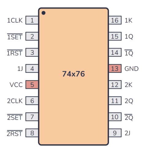
Pin Configuration and Descriptions
The 74x76 IC is a 14-pin dual in-line package (DIP). Below is the pinout and description:
| Pin Number | Pin Name | Description |
|---|---|---|
| 1 | CLR1 | Clear input for flip-flop 1 (active LOW) |
| 2 | CLK1 | Clock input for flip-flop 1 |
| 3 | J1 | J input for flip-flop 1 |
| 4 | K1 | K input for flip-flop 1 |
| 5 | Q1 | Output Q for flip-flop 1 |
| 6 | Q1̅ | Complementary output Q̅ for flip-flop 1 |
| 7 | GND | Ground (0V) |
| 8 | Q2̅ | Complementary output Q̅ for flip-flop 2 |
| 9 | Q2 | Output Q for flip-flop 2 |
| 10 | K2 | K input for flip-flop 2 |
| 11 | J2 | J input for flip-flop 2 |
| 12 | CLK2 | Clock input for flip-flop 2 |
| 13 | CLR2 | Clear input for flip-flop 2 (active LOW) |
| 14 | Vcc | Positive supply voltage (typically +5V) |
Usage Instructions
How to Use the 74x76 in a Circuit
- Power Supply: Connect pin 14 (Vcc) to a +5V power supply and pin 7 (GND) to ground.
- Inputs:
- Connect the J and K inputs (pins 3, 4 for flip-flop 1; pins 11, 10 for flip-flop 2) to the desired logic levels.
- Provide a clock signal to the CLK pins (pin 2 for flip-flop 1; pin 12 for flip-flop 2).
- Use the CLR pins (pins 1 and 13) to asynchronously reset the flip-flops if needed.
- Outputs:
- The Q and Q̅ outputs (pins 5, 6 for flip-flop 1; pins 9, 8 for flip-flop 2) provide the flip-flop states.
- Use these outputs to drive other components in your circuit.
- Logic Operation:
- The J and K inputs determine the state of the flip-flop on the rising edge of the clock signal:
- J = 0, K = 0: No change
- J = 0, K = 1: Reset (Q = 0, Q̅ = 1)
- J = 1, K = 0: Set (Q = 1, Q̅ = 0)
- J = 1, K = 1: Toggle (Q and Q̅ switch states)
- The J and K inputs determine the state of the flip-flop on the rising edge of the clock signal:
Important Considerations and Best Practices
- Debounce the Clock Signal: If the clock signal is generated by a mechanical switch, use a debouncing circuit to avoid erratic behavior.
- Avoid Floating Inputs: Always connect unused inputs (J, K, CLR) to a defined logic level (HIGH or LOW) to prevent unpredictable behavior.
- Observe Voltage Limits: Ensure the supply voltage does not exceed the specified range to avoid damaging the IC.
- Bypass Capacitor: Place a 0.1 µF ceramic capacitor close to the Vcc pin to filter out noise and stabilize the power supply.
Example: Connecting the 74x76 to an Arduino UNO
Below is an example of how to toggle a flip-flop using an Arduino UNO:
// Define pin connections
const int clockPin = 8;  // Arduino pin connected to CLK1 (pin 2 of 74x76)
const int jPin = 9;      // Arduino pin connected to J1 (pin 3 of 74x76)
const int kPin = 10;     // Arduino pin connected to K1 (pin 4 of 74x76)

void setup() {
  // Set pin modes
  pinMode(clockPin, OUTPUT);
  pinMode(jPin, OUTPUT);
  pinMode(kPin, OUTPUT);

  // Initialize J and K inputs
  digitalWrite(jPin, HIGH);  // Set J = 1
  digitalWrite(kPin, HIGH);  // Set K = 1 (toggle mode)
}

void loop() {
  // Generate a clock pulse
  digitalWrite(clockPin, HIGH);  // Set clock HIGH
  delay(10);                     // Wait for 10 ms
  digitalWrite(clockPin, LOW);   // Set clock LOW
  delay(1000);                   // Wait for 1 second before next pulse
}
Troubleshooting and FAQs
Common Issues and Solutions
Flip-Flop Not Responding to Clock Signal:
- Cause: Clock signal is not properly connected or is noisy.
- Solution: Verify the clock connection and use a debouncing circuit if necessary.
Unexpected Output States:
- Cause: Floating inputs or incorrect logic levels on J, K, or CLR pins.
- Solution: Ensure all inputs are connected to defined logic levels (HIGH or LOW).
IC Overheating:
- Cause: Supply voltage exceeds the maximum rating or excessive current draw.
- Solution: Check the power supply voltage and ensure proper current-limiting resistors are used.
Outputs Not Changing:
- Cause: CLR pin is held LOW, keeping the flip-flop in a reset state.
- Solution: Verify the CLR pin is HIGH during normal operation.
FAQs
Q1: Can I use the 74x76 with a 3.3V power supply?
A1: No, the 74x76 is designed for a 5V power supply. Using 3.3V may result in unreliable operation.
Q2: What is the difference between the 74LS76 and 74HC76?
A2: The 74LS76 is a low-power Schottky version, while the 74HC76 is a high-speed CMOS version. The 74HC76 typically has faster switching speeds and lower power consumption.
Q3: Can I cascade multiple 74x76 ICs for larger counters?
A3: Yes, you can connect the Q output of one flip-flop to the clock input of the next to create ripple counters or frequency dividers.