
How to Use AT45DB041B: Examples, Pinouts, and Specs
 Design with AT45DB041B in Cirkit Designer
Introduction
The AT45DB041B is a 4-Mbit serial Flash memory device with a Serial Peripheral Interface (SPI). It is designed for low-power applications and offers fast read and write operations, making it ideal for efficient data storage and retrieval. This component is commonly used in embedded systems, data logging, firmware storage, and other applications requiring non-volatile memory.
Explore Projects Built with AT45DB041B
 Open Project in Cirkit Designer
 Open Project in Cirkit Designer
 Open Project in Cirkit Designer
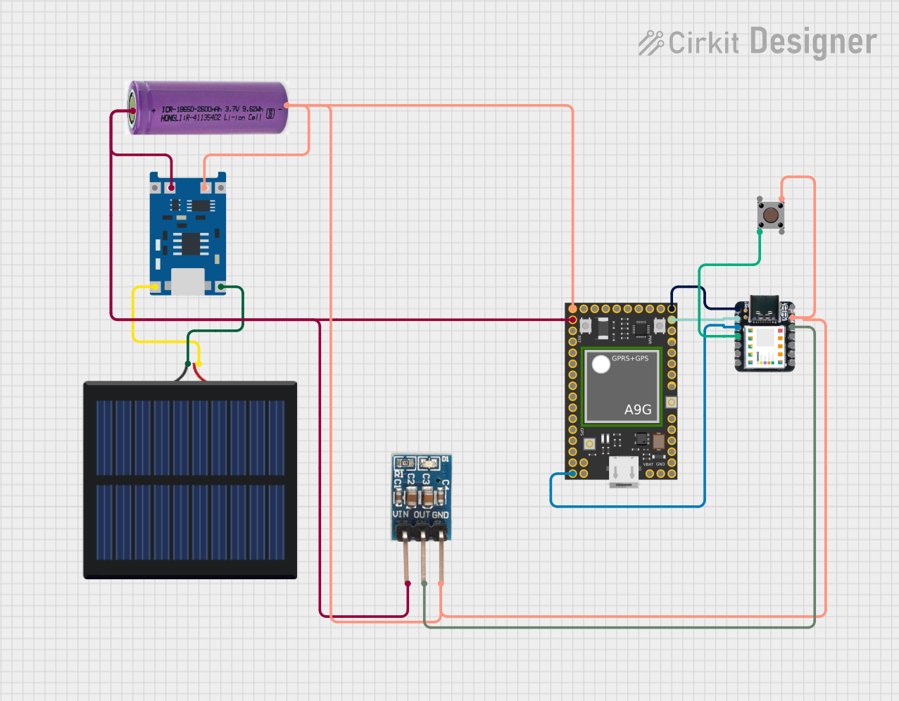 Open Project in Cirkit Designer
Explore Projects Built with AT45DB041B
Open Project in Cirkit DesignerOpen Project in Cirkit DesignerOpen Project in Cirkit DesignerOpen Project in Cirkit DesignerCommon Applications:
- Embedded systems requiring non-volatile memory
- Data logging in IoT devices
- Firmware storage for microcontrollers
- Boot memory for systems with limited onboard storage
- Portable devices requiring low-power memory solutions
Technical Specifications
Key Technical Details:
| Parameter | Value |
|---|---|
| Memory Size | 4 Mbits (512 KB) |
| Interface | SPI (Serial Peripheral Interface) |
| Operating Voltage | 2.7V to 3.6V |
| Maximum Clock Frequency | 66 MHz |
| Page Size | 264 bytes |
| Block Size | 4 KB |
| Write/Erase Endurance | 100,000 cycles (typical) |
| Data Retention | 20 years (typical) |
| Operating Temperature | -40°C to +85°C |
| Package Options | 8-pin SOIC, 8-pin DIP, etc. |
Pin Configuration and Descriptions:
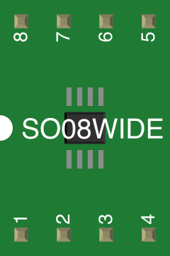
The AT45DB041B is typically available in an 8-pin package. Below is the pinout and description:
| Pin No. | Pin Name | Description |
|---|---|---|
| 1 | CS | Chip Select: Enables communication with the device when pulled low. |
| 2 | SO | Serial Output: Data output from the memory device. |
| 3 | WP | Write Protect: Protects the memory from being written when pulled low. |
| 4 | GND | Ground: Connect to system ground. |
| 5 | SI | Serial Input: Data input to the memory device. |
| 6 | SCK | Serial Clock: Clock signal for SPI communication. |
| 7 | RESET | Reset: Resets the device when pulled low. |
| 8 | VCC | Power Supply: Connect to a 2.7V to 3.6V power source. |
Usage Instructions
How to Use the AT45DB041B in a Circuit:
- Power Supply: Connect the VCC pin to a 3.3V power source and the GND pin to ground.
- SPI Communication: Connect the SCK, SI, and SO pins to the corresponding SPI pins on your microcontroller.
- Chip Select (CS): Use a GPIO pin on your microcontroller to control the CS pin. Pull it low to enable communication.
- Write Protect (WP): If write protection is not required, connect this pin to VCC.
- Reset (RESET): Connect this pin to VCC if the reset functionality is not needed.
Important Considerations:
- Ensure the SPI clock frequency does not exceed 66 MHz.
- Use decoupling capacitors (e.g., 0.1 µF) near the VCC pin to stabilize the power supply.
- Avoid exceeding the maximum write/erase cycles to ensure data integrity.
- Use the write-protect feature to prevent accidental data overwrites.
Example Code for Arduino UNO:
Below is an example of interfacing the AT45DB041B with an Arduino UNO using the SPI library:
#include <SPI.h>

// Pin definitions for the AT45DB041B
const int CS_PIN = 10; // Chip Select pin connected to Arduino pin 10

void setup() {
  // Initialize Serial Monitor for debugging
  Serial.begin(9600);

  // Initialize SPI communication
  SPI.begin();

  // Set the CS pin as output and set it high
  pinMode(CS_PIN, OUTPUT);
  digitalWrite(CS_PIN, HIGH);

  Serial.println("AT45DB041B Initialized");
}

void loop() {
  // Example: Read the device ID
  digitalWrite(CS_PIN, LOW); // Select the device
  SPI.transfer(0x9F);        // Send the "Read ID" command

  // Read the manufacturer and device ID
  byte manufacturerID = SPI.transfer(0x00);
  byte deviceID1 = SPI.transfer(0x00);
  byte deviceID2 = SPI.transfer(0x00);
  digitalWrite(CS_PIN, HIGH); // Deselect the device

  // Print the IDs to the Serial Monitor
  Serial.print("Manufacturer ID: 0x");
  Serial.println(manufacturerID, HEX);
  Serial.print("Device ID: 0x");
  Serial.print(deviceID1, HEX);
  Serial.println(deviceID2, HEX);

  delay(1000); // Wait for 1 second before repeating
}
Notes:
- Ensure the CS pin is properly toggled to enable and disable communication.
- Refer to the AT45DB041B datasheet for detailed command sequences.
Troubleshooting and FAQs
Common Issues:
No Response from the Device:
- Cause: Incorrect SPI connections or CS pin not toggled properly.
- Solution: Double-check the wiring and ensure the CS pin is pulled low during communication.
Data Corruption:
- Cause: Exceeding the write/erase endurance or power instability.
- Solution: Use decoupling capacitors and avoid frequent write/erase cycles.
Device Not Recognized:
- Cause: Incorrect SPI clock frequency or incompatible voltage levels.
- Solution: Ensure the SPI clock frequency is ≤ 66 MHz and the voltage is within 2.7V to 3.6V.
FAQs:
Q1: Can the AT45DB041B operate at 5V?
A1: No, the AT45DB041B operates within a voltage range of 2.7V to 3.6V. Use a level shifter if interfacing with a 5V system.
Q2: How do I erase data on the AT45DB041B?
A2: Use the "Block Erase" or "Chip Erase" commands as specified in the datasheet. Ensure the WP pin is not pulled low.
Q3: What is the difference between page and block operations?
A3: A page is the smallest writable unit (264 bytes), while a block consists of multiple pages (4 KB). Use block operations for faster erases.
Q4: How do I ensure data retention for 20 years?
A4: Operate the device within its specified voltage and temperature ranges, and avoid exceeding the write/erase endurance.