
How to Use SN74LS32N: Examples, Pinouts, and Specs
 Design with SN74LS32N in Cirkit Designer
Introduction
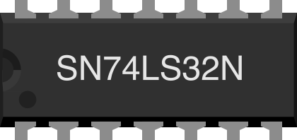
The SN74LS32N is a quad 2-input OR gate, manufactured by Texas Instruments. It is part of the 74LS series of TTL (Transistor-Transistor Logic) integrated circuits. This IC contains four independent OR gates, each capable of accepting two inputs and providing a single output. Designed for high-speed operation and low power consumption, the SN74LS32N is widely used in digital logic applications.
Explore Projects Built with SN74LS32N
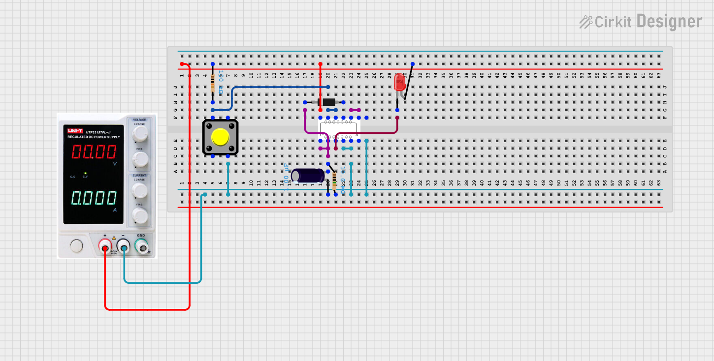 Open Project in Cirkit Designer
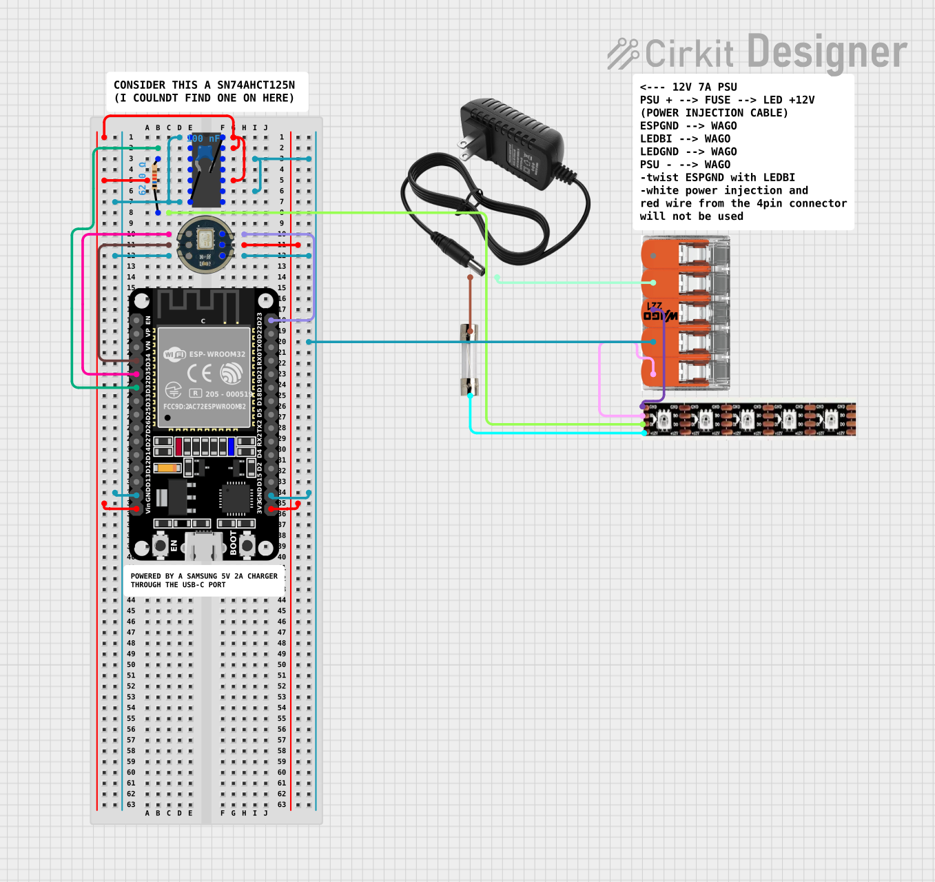 Open Project in Cirkit Designer
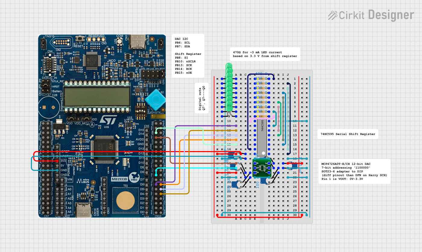 Open Project in Cirkit Designer
 Open Project in Cirkit Designer
Explore Projects Built with SN74LS32N
Open Project in Cirkit DesignerOpen Project in Cirkit DesignerOpen Project in Cirkit DesignerOpen Project in Cirkit DesignerCommon Applications
- Digital signal processing
- Logic level conversion
- Data routing and control
- Arithmetic and logic operations in digital systems
- General-purpose logic circuits
Technical Specifications
Key Technical Details
| Parameter | Value |
|---|---|
| Supply Voltage (Vcc) | 4.75V to 5.25V |
| Input Voltage (VI) | 0V to 7V |
| High-Level Output Voltage (VOH) | 2.7V (min) at 0.4mA load |
| Low-Level Output Voltage (VOL) | 0.4V (max) at 8mA load |
| High-Level Input Current (IIH) | 20µA (max) |
| Low-Level Input Current (IIL) | -0.4mA (max) |
| Propagation Delay (tpd) | 9ns (typical) |
| Power Dissipation | 20mW (typical) |
| Operating Temperature | 0°C to 70°C |
| Package Type | DIP-14 (Dual Inline Package, 14 pins) |
Pin Configuration and Descriptions
The SN74LS32N comes in a 14-pin DIP package. The pinout is as follows:
| Pin Number | Pin Name | Description |
|---|---|---|
| 1 | 1A | Input A for OR Gate 1 |
| 2 | 1B | Input B for OR Gate 1 |
| 3 | 1Y | Output Y for OR Gate 1 |
| 4 | 2A | Input A for OR Gate 2 |
| 5 | 2B | Input B for OR Gate 2 |
| 6 | 2Y | Output Y for OR Gate 2 |
| 7 | GND | Ground (0V) |
| 8 | 3A | Input A for OR Gate 3 |
| 9 | 3B | Input B for OR Gate 3 |
| 10 | 3Y | Output Y for OR Gate 3 |
| 11 | 4A | Input A for OR Gate 4 |
| 12 | 4B | Input B for OR Gate 4 |
| 13 | 4Y | Output Y for OR Gate 4 |
| 14 | Vcc | Positive Supply Voltage (+5V) |
Usage Instructions
How to Use the SN74LS32N in a Circuit
- Power Supply: Connect pin 14 (Vcc) to a +5V power supply and pin 7 (GND) to ground.
- Inputs: Provide digital logic signals (HIGH or LOW) to the input pins (1A, 1B, 2A, 2B, etc.).
- Outputs: The output pins (1Y, 2Y, 3Y, 4Y) will provide the logical OR of the corresponding input pairs.
- Load Considerations: Ensure the output load does not exceed the maximum current rating to avoid damage.
Important Considerations
- Decoupling Capacitor: Place a 0.1µF ceramic capacitor close to the Vcc pin to filter noise and stabilize the power supply.
- Unused Inputs: Tie unused inputs to GND or Vcc to prevent floating inputs, which can cause erratic behavior.
- Voltage Levels: Ensure input voltage levels are within the specified range (0V to 7V) to avoid damage to the IC.
Example: Connecting SN74LS32N to an Arduino UNO
The SN74LS32N can be used with an Arduino UNO to perform basic logic operations. Below is an example of how to use the IC to implement an OR gate:
Circuit Connections
- Connect pin 14 (Vcc) to the Arduino's 5V pin.
- Connect pin 7 (GND) to the Arduino's GND pin.
- Connect two Arduino digital pins (e.g., D2 and D3) to inputs 1A and 1B.
- Connect the output 1Y (pin 3) to another Arduino digital pin (e.g., D4) for reading the result.
Arduino Code
// Define input and output pins
const int inputA = 2;  // Input A connected to Arduino pin D2
const int inputB = 3;  // Input B connected to Arduino pin D3
const int outputY = 4; // Output Y connected to Arduino pin D4

void setup() {
  // Set input pins as OUTPUT to drive the SN74LS32N inputs
  pinMode(inputA, OUTPUT);
  pinMode(inputB, OUTPUT);

  // Set output pin as INPUT to read the OR gate output
  pinMode(outputY, INPUT);

  // Initialize Serial Monitor for debugging
  Serial.begin(9600);
}

void loop() {
  // Example: Test OR gate with different input combinations
  digitalWrite(inputA, LOW);  // Set Input A to LOW
  digitalWrite(inputB, HIGH); // Set Input B to HIGH

  // Read the output of the OR gate
  int result = digitalRead(outputY);

  // Print the result to the Serial Monitor
  Serial.print("Input A: LOW, Input B: HIGH, Output Y: ");
  Serial.println(result == HIGH ? "HIGH" : "LOW");

  delay(1000); // Wait for 1 second before the next test
}
Troubleshooting and FAQs
Common Issues and Solutions
No Output Signal:
- Ensure the power supply is properly connected to Vcc (pin 14) and GND (pin 7).
- Verify that the input signals are within the specified voltage range.
- Check for loose or incorrect wiring.
Erratic Behavior:
- Add a decoupling capacitor (0.1µF) near the Vcc pin to stabilize the power supply.
- Tie unused inputs to GND or Vcc to prevent floating inputs.
Overheating:
- Ensure the output load does not exceed the maximum current rating.
- Verify that the IC is operating within the recommended temperature range.
FAQs
Q1: Can the SN74LS32N operate at 3.3V?
A1: No, the SN74LS32N is designed for a supply voltage range of 4.75V to 5.25V. For 3.3V operation, consider using a CMOS-based OR gate like the 74HC32.
Q2: What happens if I leave an input pin floating?
A2: Floating inputs can cause unpredictable behavior. Always tie unused inputs to GND or Vcc.
Q3: Can I use the SN74LS32N for high-frequency applications?
A3: The SN74LS32N has a typical propagation delay of 9ns, making it suitable for moderate-speed applications. For higher frequencies, consider faster logic families like the 74F series.
Q4: Is the SN74LS32N compatible with CMOS logic levels?
A4: The SN74LS32N is a TTL device and may not be directly compatible with CMOS logic levels. Use level shifters if interfacing with CMOS circuits.