
How to Use OP482 - Low Power, High Speed JFET Quad Operational Amplifier: Examples, Pinouts, and Specs
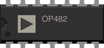
 Design with OP482 - Low Power, High Speed JFET Quad Operational Amplifier in Cirkit Designer
Introduction
The OP482 is a quad operational amplifier manufactured by Analog Devices, with the part ID OP482GPZ. This component is designed to deliver high-speed performance while maintaining low power consumption. It features JFET input stages, which provide high input impedance and low noise, making it ideal for precision applications. The OP482 is commonly used in signal processing, instrumentation, active filters, and data acquisition systems.
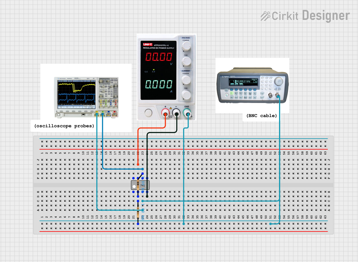
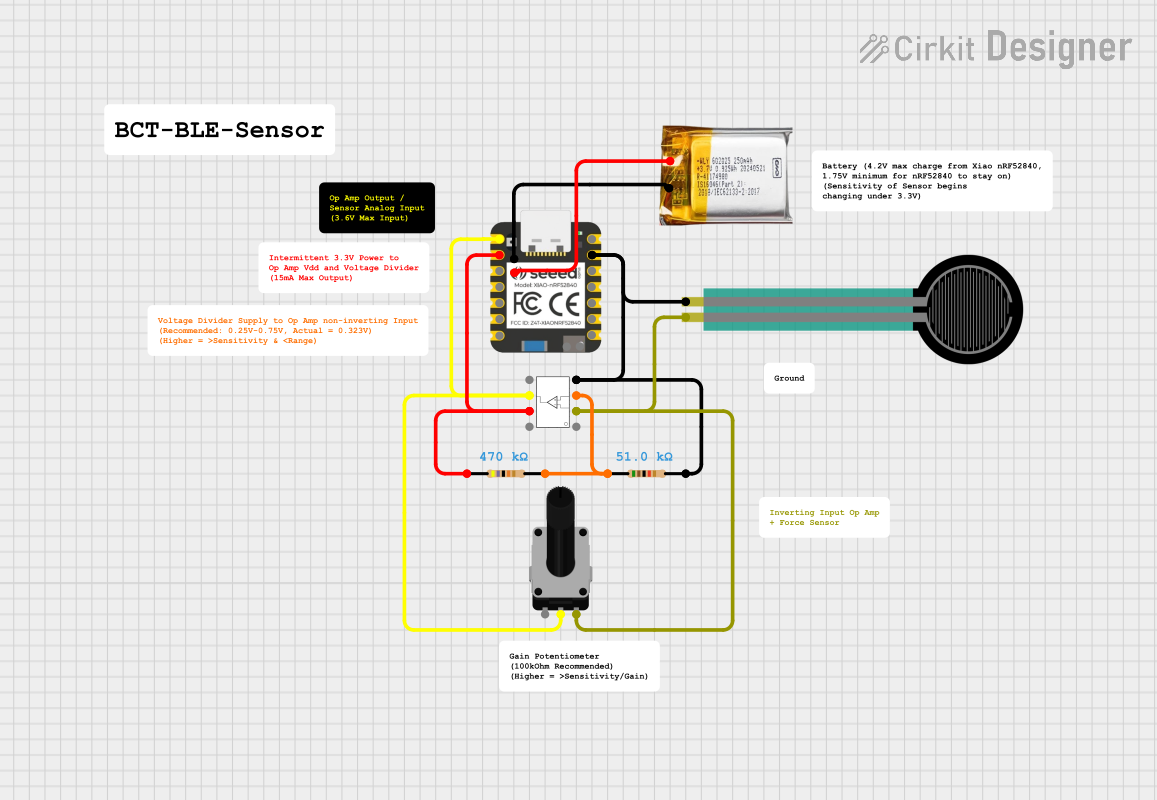
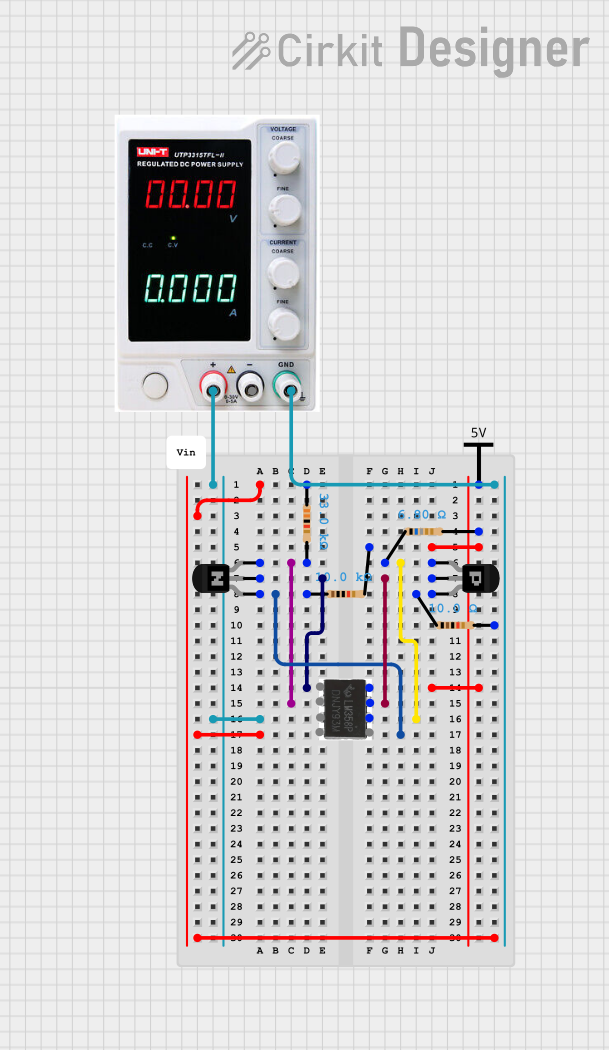
Explore Projects Built with OP482 - Low Power, High Speed JFET Quad Operational Amplifier
 Open Project in Cirkit Designer
 Open Project in Cirkit Designer
 Open Project in Cirkit Designer
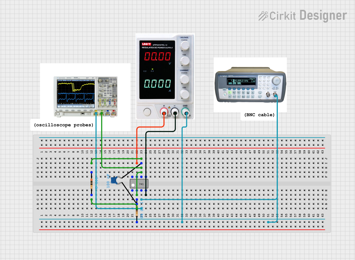 Open Project in Cirkit Designer
Explore Projects Built with OP482 - Low Power, High Speed JFET Quad Operational Amplifier
Open Project in Cirkit DesignerOpen Project in Cirkit DesignerOpen Project in Cirkit DesignerOpen Project in Cirkit DesignerCommon Applications:
- Signal conditioning and processing
- Active filters and integrators
- Data acquisition systems
- Precision instrumentation
- Low-noise audio applications
Technical Specifications
The OP482 is a high-performance operational amplifier with the following key specifications:
| Parameter | Value |
|---|---|
| Supply Voltage Range | ±2 V to ±18 V |
| Input Offset Voltage | 0.5 mV (typical) |
| Input Bias Current | 10 pA (typical) |
| Slew Rate | 9 V/µs (typical) |
| Gain Bandwidth Product | 4 MHz |
| Supply Current (per amplifier) | 1.2 mA (typical) |
| Input Impedance | 10⁹ Ω (typical) |
| Output Voltage Swing | ±13.5 V (with ±15 V supply) |
| Operating Temperature Range | -40°C to +85°C |
| Package Type | 14-pin PDIP (Plastic Dual Inline Package) |
Pin Configuration and Descriptions
The OP482 is available in a 14-pin PDIP package. The pinout and descriptions are as follows:
| Pin Number | Pin Name | Description |
|---|---|---|
| 1 | OUT A | Output of Amplifier A |
| 2 | IN A- | Inverting Input of Amplifier A |
| 3 | IN A+ | Non-Inverting Input of Amplifier A |
| 4 | V+ | Positive Power Supply |
| 5 | IN B+ | Non-Inverting Input of Amplifier B |
| 6 | IN B- | Inverting Input of Amplifier B |
| 7 | OUT B | Output of Amplifier B |
| 8 | OUT C | Output of Amplifier C |
| 9 | IN C- | Inverting Input of Amplifier C |
| 10 | IN C+ | Non-Inverting Input of Amplifier C |
| 11 | V- | Negative Power Supply (Ground in single-supply) |
| 12 | IN D+ | Non-Inverting Input of Amplifier D |
| 13 | IN D- | Inverting Input of Amplifier D |
| 14 | OUT D | Output of Amplifier D |
Usage Instructions
How to Use the OP482 in a Circuit
- Power Supply: Connect the OP482 to a dual power supply (e.g., ±15 V) or a single power supply (e.g., 5 V to 36 V). Ensure the supply voltage does not exceed the specified range of ±18 V.
- Input Connections: Use the inverting (
IN-) and non-inverting (IN+) inputs of each amplifier as required by your circuit design. - Output Connections: Connect the output pins (
OUT) to the desired load or subsequent circuit stage. Ensure the load impedance is within the recommended range to avoid distortion. - Bypass Capacitors: Place decoupling capacitors (e.g., 0.1 µF ceramic and 10 µF electrolytic) close to the power supply pins to minimize noise and ensure stable operation.
- Feedback Network: Design the feedback network (resistors and capacitors) based on the desired gain and frequency response of your application.
Important Considerations and Best Practices
- Input Protection: Avoid applying voltages beyond the supply rails to the input pins to prevent damage.
- Thermal Management: Ensure adequate ventilation or heat dissipation if the device operates in high-temperature environments.
- Stability: Use proper compensation techniques if the amplifier is used in high-gain configurations to prevent oscillations.
- Unused Amplifiers: If any of the four amplifiers are unused, configure them as voltage followers (connect
IN+to a reference voltage andIN-to the output) to avoid noise interference.
Example: Connecting OP482 to an Arduino UNO
The OP482 can be used with an Arduino UNO for signal amplification or conditioning. Below is an example of using the OP482 to amplify an analog signal:
Circuit Setup:
- Connect the OP482's
V+to +5 V andV-to GND. - Connect the signal source to the non-inverting input (
IN A+) of Amplifier A. - Use a resistor network to set the desired gain (e.g., 10x).
- Connect the output (
OUT A) to an analog input pin (e.g., A0) of the Arduino UNO.
Arduino Code Example:
// Example code to read an amplified signal from OP482 and display it via Serial Monitor

const int analogPin = A0; // Analog pin connected to OP482 output

void setup() {
  Serial.begin(9600); // Initialize serial communication at 9600 baud
}

void loop() {
  int sensorValue = analogRead(analogPin); // Read the analog value (0-1023)

  // Convert the analog value to voltage (assuming 5V reference)
  float voltage = sensorValue * (5.0 / 1023.0);

  // Print the voltage to the Serial Monitor
  Serial.print("Amplified Signal Voltage: ");
  Serial.print(voltage);
  Serial.println(" V");

  delay(500); // Wait for 500 ms before the next reading
}
Troubleshooting and FAQs
Common Issues and Solutions
No Output Signal:
- Cause: Incorrect power supply connections.
- Solution: Verify the power supply polarity and voltage levels.
Distorted Output:
- Cause: Load impedance too low or incorrect feedback network.
- Solution: Ensure the load impedance is within the recommended range and check the feedback network design.
Oscillations or Noise:
- Cause: Insufficient power supply decoupling or improper layout.
- Solution: Add bypass capacitors close to the power pins and ensure a proper PCB layout.
High Input Offset Voltage:
- Cause: Mismatched input impedance or temperature variations.
- Solution: Use precision resistors and consider temperature compensation techniques.
FAQs
Q1: Can the OP482 operate with a single power supply?
A1: Yes, the OP482 can operate with a single supply voltage ranging from 5 V to 36 V. Connect V- to GND in single-supply configurations.
Q2: What is the maximum gain I can achieve with the OP482?
A2: The maximum gain depends on the feedback network and the stability of the circuit. For high-gain applications, ensure proper compensation to avoid oscillations.
Q3: Is the OP482 suitable for audio applications?
A3: Yes, the OP482's low noise and high input impedance make it suitable for low-noise audio amplification.
Q4: How do I handle unused amplifiers in the OP482?
A4: Configure unused amplifiers as voltage followers to minimize noise and interference.