How to Use HMC253 RF-Multiplexer: Examples, Pinouts, and Specs
Introduction
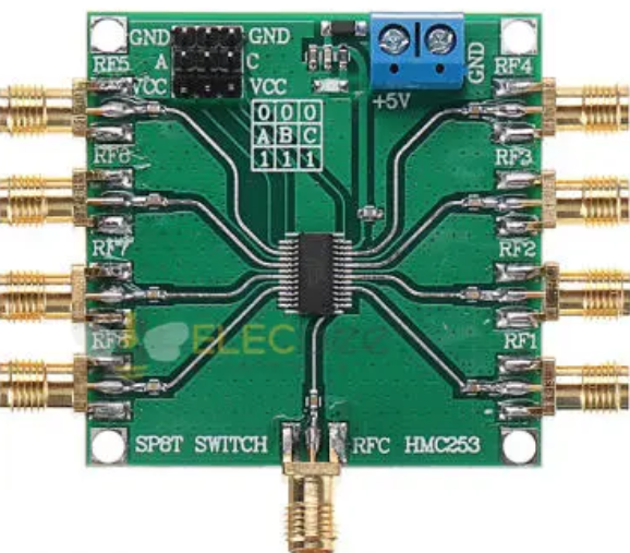
The HMC253 is a high-performance RF multiplexer designed for switching RF signals in communication systems. It is a versatile component that offers low insertion loss, high isolation, and a wide frequency range of operation. These features make it an ideal choice for applications in wireless communication systems, satellite communications, and test equipment.
Explore Projects Built with HMC253 RF-Multiplexer
Explore Projects Built with HMC253 RF-Multiplexer
Common Applications and Use Cases
- Wireless communication systems (e.g., base stations, repeaters)
- Satellite communication systems
- RF signal routing in test and measurement equipment
- Antenna switching in multi-band systems
- General-purpose RF signal switching in laboratory setups
Technical Specifications
The HMC253 RF multiplexer is designed to meet the demanding requirements of RF signal switching. Below are its key technical specifications:
| Parameter | Value |
|---|---|
| Frequency Range | DC to 3 GHz |
| Insertion Loss | 1.5 dB (typical) |
| Isolation | 40 dB (typical) |
| Input Power for 1 dB Compression | +25 dBm |
| Control Voltage Range | 0 V to +5 V |
| Supply Voltage | +5 V |
| Operating Temperature Range | -40°C to +85°C |
| Package Type | 16-lead SMT package |
Pin Configuration and Descriptions
The HMC253 is housed in a 16-lead surface-mount package. Below is the pin configuration and description:
| Pin Number | Pin Name | Description |
|---|---|---|
| 1 | RF1 | RF Input/Output Port 1 |
| 2 | RF2 | RF Input/Output Port 2 |
| 3 | RF3 | RF Input/Output Port 3 |
| 4 | RF4 | RF Input/Output Port 4 |
| 5 | GND | Ground |
| 6 | VDD | Supply Voltage (+5 V) |
| 7 | CTRL1 | Control Input 1 |
| 8 | CTRL2 | Control Input 2 |
| 9 | CTRL3 | Control Input 3 |
| 10 | GND | Ground |
| 11 | RF5 | RF Input/Output Port 5 |
| 12 | RF6 | RF Input/Output Port 6 |
| 13 | RF7 | RF Input/Output Port 7 |
| 14 | RF8 | RF Input/Output Port 8 |
| 15 | GND | Ground |
| 16 | NC | No Connection |
Usage Instructions
The HMC253 RF multiplexer is straightforward to use in RF signal switching applications. Below are the steps and considerations for integrating it into a circuit:
How to Use the Component in a Circuit
- Power Supply: Connect the VDD pin to a +5 V DC power supply and ensure all GND pins are connected to the ground plane of the PCB.
- Control Inputs: Use the CTRL1, CTRL2, and CTRL3 pins to control the switching state of the multiplexer. These pins accept logic levels (0 V or +5 V) to select the desired RF path.
- RF Connections: Connect the RF input/output ports (RF1 to RF8) to the desired RF signal paths. Ensure proper impedance matching (typically 50 ohms) for optimal performance.
- Bypass Capacitors: Place decoupling capacitors (e.g., 0.01 µF) close to the VDD pin to filter out noise and ensure stable operation.
Important Considerations and Best Practices
- Impedance Matching: Ensure all RF ports are properly impedance-matched to 50 ohms to minimize signal reflections and maximize performance.
- Control Logic: Use a microcontroller or logic circuit to generate the control signals for the CTRL pins. Ensure the control voltage levels are within the specified range (0 V to +5 V).
- Thermal Management: Operate the component within the specified temperature range (-40°C to +85°C) to avoid performance degradation.
- PCB Design: Use a high-frequency PCB design with proper grounding and trace layout to minimize signal loss and crosstalk.
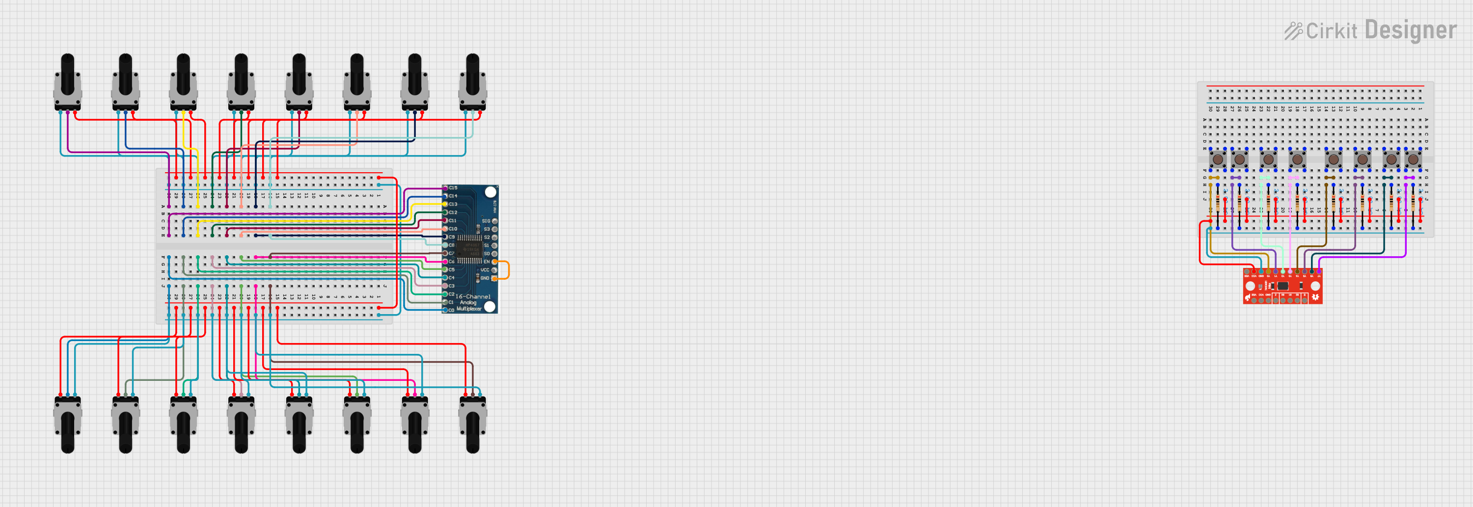
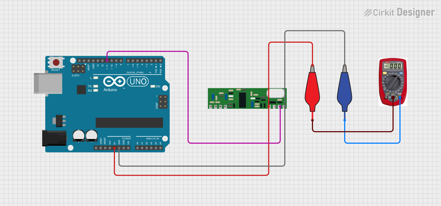
Example: Connecting to an Arduino UNO
The HMC253 can be controlled using an Arduino UNO to switch between RF paths. Below is an example code snippet:
// Define control pins connected to Arduino
const int ctrl1 = 2; // Connect CTRL1 to Arduino pin 2
const int ctrl2 = 3; // Connect CTRL2 to Arduino pin 3
const int ctrl3 = 4; // Connect CTRL3 to Arduino pin 4

void setup() {
  // Set control pins as outputs
  pinMode(ctrl1, OUTPUT);
  pinMode(ctrl2, OUTPUT);
  pinMode(ctrl3, OUTPUT);
}

void loop() {
  // Example: Select RF path 1
  digitalWrite(ctrl1, LOW); // Set CTRL1 to 0
  digitalWrite(ctrl2, LOW); // Set CTRL2 to 0
  digitalWrite(ctrl3, LOW); // Set CTRL3 to 0
  delay(1000); // Wait for 1 second

  // Example: Select RF path 2
  digitalWrite(ctrl1, HIGH); // Set CTRL1 to 1
  digitalWrite(ctrl2, LOW);  // Set CTRL2 to 0
  digitalWrite(ctrl3, LOW);  // Set CTRL3 to 0
  delay(1000); // Wait for 1 second

  // Add more control logic as needed for other RF paths
}
Troubleshooting and FAQs
Common Issues Users Might Face
- High Insertion Loss: If the insertion loss is higher than expected, check for proper impedance matching and ensure the RF traces are designed for high-frequency signals.
- Control Signal Malfunction: If the RF paths are not switching correctly, verify the control signal levels and connections to the CTRL pins.
- Noise or Signal Distortion: Ensure proper grounding and use bypass capacitors to filter out noise from the power supply.
Solutions and Tips for Troubleshooting
- Verify Connections: Double-check all connections, especially the control pins and RF ports.
- Test Control Signals: Use an oscilloscope to confirm the control signals are within the specified voltage range.
- Inspect PCB Design: Ensure the PCB layout follows high-frequency design practices, such as minimizing trace lengths and using a solid ground plane.
- Check Power Supply: Ensure the supply voltage is stable and within the specified range (+5 V).
By following these guidelines and best practices, the HMC253 RF multiplexer can be effectively integrated into a wide range of RF applications.