How to Use CD74HC4067_16CH_MUX: Examples, Pinouts, and Specs
Introduction
The CD74HC4067 is a 16-channel analog multiplexer/demultiplexer that enables the selection of one of 16 input channels to connect to a single output line. This selection is controlled using a 4-bit binary address. The component is highly versatile and is commonly used in applications requiring signal routing, data acquisition, or expansion of input/output capabilities in microcontroller-based systems.
Explore Projects Built with CD74HC4067_16CH_MUX

Explore Projects Built with CD74HC4067_16CH_MUX
Common Applications
- Signal multiplexing in data acquisition systems
- Expanding analog or digital input/output ports
- Sensor arrays and matrix keypads
- Audio signal routing
- Microcontroller-based projects (e.g., Arduino, Raspberry Pi)
Technical Specifications
The CD74HC4067 is a high-speed CMOS device with the following key specifications:
| Parameter | Value |
|---|---|
| Supply Voltage (Vcc) | 2V to 6V |
| Input Voltage Range | 0V to Vcc |
| Maximum Current per Pin | ±25mA |
| On-Resistance (Ron) | ~70Ω (typical at 5V Vcc) |
| Propagation Delay | ~10ns (typical at 5V Vcc) |
| Operating Temperature Range | -55°C to +125°C |
| Package Types | DIP, SOIC, TSSOP |
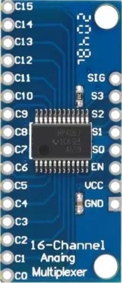
Pin Configuration and Descriptions
The CD74HC4067 has 24 pins, with the following configuration:
| Pin Number | Pin Name | Description |
|---|---|---|
| 1-16 | CH0-CH15 | Analog or digital input/output channels (multiplexed to the COM pin) |
| 23 | COM | Common I/O pin (connected to one of CH0-CH15 based on the address selection) |
| 10, 11, 12, 13 | S0, S1, S2, S3 | Address selection pins (4-bit binary input to select one of 16 channels) |
| 24 | Vcc | Positive power supply (2V to 6V) |
| 12 | GND | Ground |
| 15 | EN | Enable pin (active LOW; when HIGH, all channels are disconnected) |
Usage Instructions
How to Use the CD74HC4067 in a Circuit
- Power Supply: Connect the Vcc pin to a voltage source (2V to 6V) and the GND pin to ground.
- Channel Selection: Use the S0-S3 pins to provide a 4-bit binary address to select one of the 16 channels (CH0-CH15). For example:
- Address
0000selects CH0. - Address
1111selects CH15.
- Address
- Enable Pin: Ensure the EN pin is set to LOW to enable the multiplexer. If EN is HIGH, all channels are disconnected.
- Signal Routing: Connect the signal source or destination to the COM pin. The selected channel will be routed to this pin.
Important Considerations
- Voltage Levels: Ensure that the input signal voltage does not exceed the supply voltage (Vcc).
- On-Resistance: The on-resistance (Ron) of the multiplexer can introduce a small voltage drop, especially at higher currents.
- Decoupling Capacitor: Place a decoupling capacitor (e.g., 0.1µF) near the Vcc pin to stabilize the power supply.
- Unused Pins: Leave unused channels (CHx) floating or connect them to ground through a pull-down resistor to avoid noise.
Example: Connecting to an Arduino UNO
The following example demonstrates how to use the CD74HC4067 with an Arduino UNO to read analog signals from multiple sensors.
Circuit Connections
- Connect Vcc to the Arduino's 5V pin and GND to the Arduino's GND.
- Connect the COM pin to the Arduino's A0 analog input.
- Connect S0-S3 to Arduino digital pins 2, 3, 4, and 5, respectively.
- Connect the EN pin to GND to enable the multiplexer.
- Connect sensors to CH0-CH15.
Arduino Code
// Define the address selection pins
const int S0 = 2;
const int S1 = 3;
const int S2 = 4;
const int S3 = 5;

// Define the analog input pin for the COM pin
const int COM_PIN = A0;

void setup() {
  // Set the address pins as outputs
  pinMode(S0, OUTPUT);
  pinMode(S1, OUTPUT);
  pinMode(S2, OUTPUT);
  pinMode(S3, OUTPUT);

  // Initialize serial communication for debugging
  Serial.begin(9600);
}

void loop() {
  for (int channel = 0; channel < 16; channel++) {
    // Set the address pins to select the desired channel
    digitalWrite(S0, channel & 0x01); // Set S0 to the least significant bit
    digitalWrite(S1, (channel >> 1) & 0x01); // Set S1 to the second bit
    digitalWrite(S2, (channel >> 2) & 0x01); // Set S2 to the third bit
    digitalWrite(S3, (channel >> 3) & 0x01); // Set S3 to the most significant bit

    // Read the analog value from the selected channel
    int sensorValue = analogRead(COM_PIN);

    // Print the channel number and sensor value to the serial monitor
    Serial.print("Channel ");
    Serial.print(channel);
    Serial.print(": ");
    Serial.println(sensorValue);

    // Wait for a short delay before reading the next channel
    delay(100);
  }
}
Troubleshooting and FAQs
Common Issues
No Signal Output on COM Pin:
- Ensure the EN pin is set to LOW.
- Verify that the address pins (S0-S3) are correctly configured.
Incorrect Channel Selection:
- Double-check the binary address provided to the S0-S3 pins.
- Ensure the Arduino code or external logic is correctly setting the address.
Signal Distortion or Voltage Drop:
- Check if the input signal exceeds the supply voltage (Vcc).
- Consider the on-resistance (Ron) of the multiplexer and its effect on high-current signals.
Noise or Unstable Readings:
- Use pull-down resistors on unused channels.
- Add a decoupling capacitor near the Vcc pin.
FAQs
Q: Can the CD74HC4067 handle digital signals?
A: Yes, the CD74HC4067 can handle both analog and digital signals, as long as the signal voltage is within the supply voltage range (0V to Vcc).
Q: What happens if the EN pin is left floating?
A: If the EN pin is left floating, its state may be undefined, leading to unpredictable behavior. Always connect it to GND (LOW) to enable the multiplexer or to Vcc (HIGH) to disable it.
Q: Can multiple CD74HC4067 chips be cascaded?
A: Yes, multiple chips can be cascaded to expand the number of channels. Use additional address lines or logic to control the enable pins of each chip.
Q: What is the maximum frequency the CD74HC4067 can handle?
A: The maximum frequency depends on the supply voltage and the load capacitance. For typical applications, it can handle signals up to a few MHz.