
How to Use AD7781: Examples, Pinouts, and Specs
 Design with AD7781 in Cirkit Designer
Introduction
The AD7781 is a low-power, 24-bit sigma-delta analog-to-digital converter (ADC) manufactured by Analog Devices. It is designed for high-precision measurement applications, offering exceptional performance in a compact package. The AD7781 features an integrated programmable gain amplifier (PGA) and operates via a simple serial interface, making it ideal for applications requiring accurate and reliable data acquisition.
Explore Projects Built with AD7781
 Open Project in Cirkit Designer
 Open Project in Cirkit Designer
 Open Project in Cirkit Designer
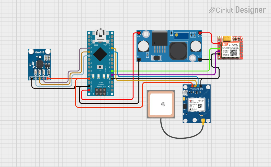 Open Project in Cirkit Designer
Explore Projects Built with AD7781
Open Project in Cirkit DesignerOpen Project in Cirkit DesignerOpen Project in Cirkit DesignerOpen Project in Cirkit DesignerCommon Applications
- Weigh scales
- Industrial process control
- Temperature measurement systems
- Pressure sensors
- Medical instrumentation
Technical Specifications
Key Technical Details
| Parameter | Value |
|---|---|
| Resolution | 24-bit |
| Input Type | Differential |
| Supply Voltage | 2.7 V to 5.25 V |
| Power Consumption | 330 µA (typical) |
| Input Voltage Range | ±VREF/Gain |
| Programmable Gain Settings | 1, 2, 4, 8, 16, 32, 64, 128 |
| Reference Voltage Range | 0.1 V to AVDD |
| Output Data Rate | Up to 16.6 Hz |
| Interface Type | Serial Peripheral Interface (SPI) |
| Operating Temperature | -40°C to +105°C |
| Package Type | 16-lead TSSOP |
Pin Configuration and Descriptions
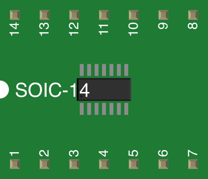
The AD7781 is available in a 16-lead TSSOP package. Below is the pin configuration and description:
| Pin No. | Pin Name | Description |
|---|---|---|
| 1 | AVDD | Analog power supply (2.7 V to 5.25 V). |
| 2 | REFIN(+) | Positive reference input. |
| 3 | REFIN(-) | Negative reference input. |
| 4 | AIN(+) | Positive analog input. |
| 5 | AIN(-) | Negative analog input. |
| 6 | GND | Ground reference. |
| 7 | SCLK | Serial clock input for SPI communication. |
| 8 | DIN | Serial data input for SPI communication. |
| 9 | DOUT/RDY | Serial data output and data ready signal. |
| 10 | CS | Chip select input (active low). |
| 11-16 | NC | No connection (leave unconnected or connect to ground for stability). |
Usage Instructions
How to Use the AD7781 in a Circuit
- Power Supply: Connect the AVDD pin to a stable power supply (2.7 V to 5.25 V) and the GND pin to the ground.
- Reference Voltage: Provide a stable reference voltage between the REFIN(+) and REFIN(-) pins. The reference voltage determines the input voltage range.
- Analog Input: Connect the differential analog input signal to the AIN(+) and AIN(-) pins. Ensure the input voltage does not exceed the specified range (±VREF/Gain).
- SPI Communication:
- Connect the SCLK, DIN, DOUT/RDY, and CS pins to the corresponding SPI pins of a microcontroller or processor.
- Use the SPI interface to configure the ADC and read data.
- Bypass Capacitors: Place decoupling capacitors (e.g., 0.1 µF and 10 µF) close to the AVDD and REFIN pins to reduce noise.
Important Considerations
- Input Impedance: The AD7781 has a high input impedance, but ensure the source impedance is low enough to avoid signal degradation.
- Noise Reduction: Use proper grounding and shielding techniques to minimize noise in precision applications.
- Data Rate: The output data rate is inversely proportional to the resolution. Choose a data rate that balances speed and accuracy for your application.
Example: Connecting the AD7781 to an Arduino UNO
Below is an example of how to interface the AD7781 with an Arduino UNO using SPI:
Circuit Connections
| AD7781 Pin | Arduino UNO Pin |
|---|---|
| AVDD | 5V |
| GND | GND |
| SCLK | D13 (SCK) |
| DIN | D11 (MOSI) |
| DOUT/RDY | D12 (MISO) |
| CS | D10 (SS) |
Arduino Code
#include <SPI.h>

// Define AD7781 pins
const int CS_PIN = 10; // Chip Select pin

void setup() {
  // Initialize SPI communication
  SPI.begin();
  pinMode(CS_PIN, OUTPUT);
  digitalWrite(CS_PIN, HIGH); // Set CS high to deselect the AD7781

  Serial.begin(9600); // Initialize serial communication for debugging
}

void loop() {
  // Select the AD7781
  digitalWrite(CS_PIN, LOW);

  // Read data from the AD7781
  uint32_t adcData = 0;
  for (int i = 0; i < 3; i++) {
    adcData = (adcData << 8) | SPI.transfer(0x00);
    // Shift the data left and read one byte at a time
  }

  // Deselect the AD7781
  digitalWrite(CS_PIN, HIGH);

  // Print the 24-bit ADC data
  Serial.print("ADC Data: ");
  Serial.println(adcData, HEX);

  delay(1000); // Wait for 1 second before the next reading
}
Troubleshooting and FAQs
Common Issues and Solutions
No Data Output:
- Ensure the SPI connections are correct and the CS pin is properly toggled.
- Verify the power supply and reference voltage are within the specified range.
Unstable Readings:
- Check for noise in the power supply or reference voltage.
- Use proper decoupling capacitors and grounding techniques.
Incorrect Data:
- Verify the SPI clock polarity and phase settings. The AD7781 requires SPI Mode 3 (CPOL = 1, CPHA = 1).
- Ensure the input signal is within the specified range.
FAQs
Q: Can the AD7781 operate with a single-ended input?
A: No, the AD7781 is designed for differential input signals. For single-ended signals, use a differential amplifier to convert the signal.
Q: What is the maximum sampling rate of the AD7781?
A: The maximum output data rate is 16.6 Hz, which is suitable for precision applications.
Q: How do I reduce noise in my measurements?
A: Use proper shielding, grounding, and bypass capacitors. Additionally, operate the ADC in a low-noise environment and minimize external interference.
Q: Can I use the AD7781 with a 3.3 V microcontroller?
A: Yes, the AD7781 operates with a supply voltage as low as 2.7 V, making it compatible with 3.3 V systems. Ensure the SPI voltage levels are compatible.