How to Use PCB: Examples, Pinouts, and Specs
Introduction
A Printed Circuit Board (PCB) is a flat board made of insulating material that holds and connects electronic components using conductive pathways, tracks, or signal traces. PCBs are essential in modern electronics, providing a compact and reliable platform for assembling and interconnecting components.
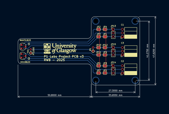
Manufactured by Glasgow University, this PCB is designed to meet high-quality standards, ensuring durability and precision in various electronic applications. PCBs are widely used in consumer electronics, industrial equipment, medical devices, and more.
Explore Projects Built with PCB
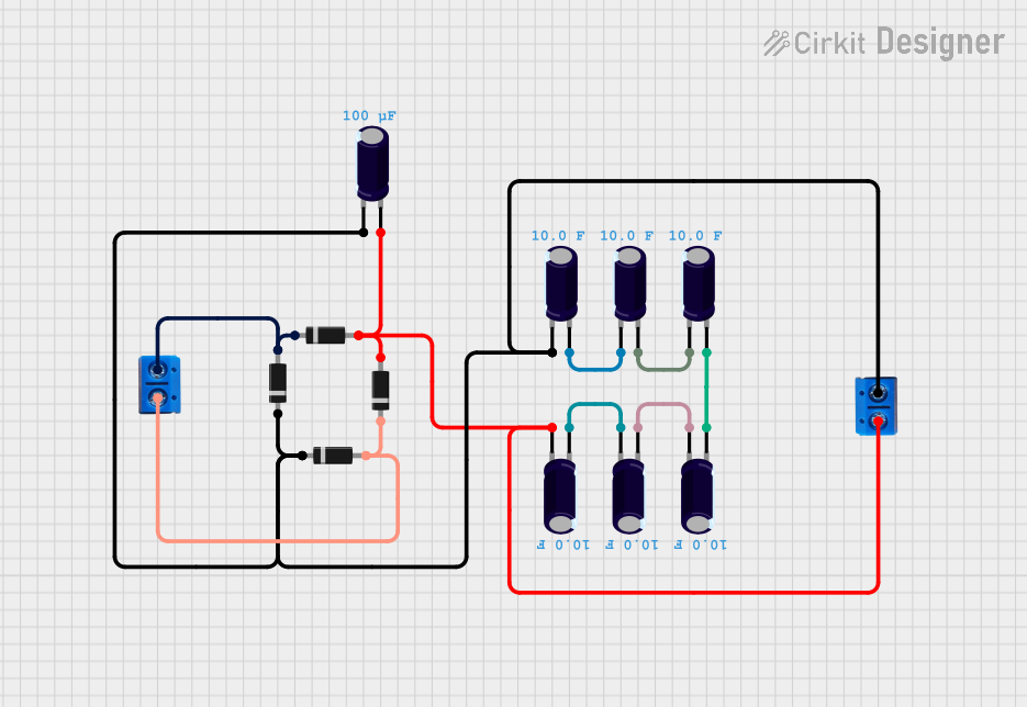
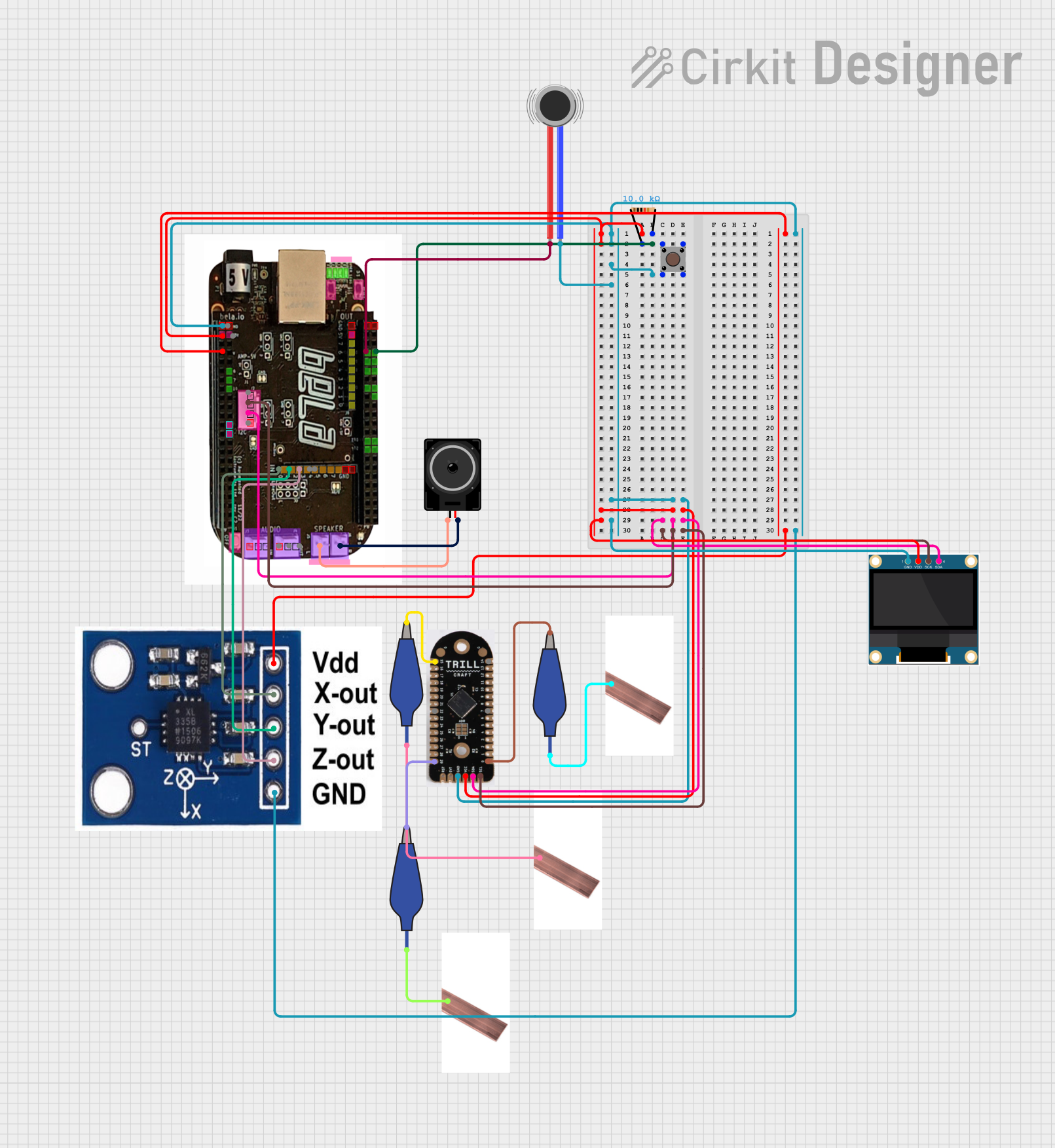
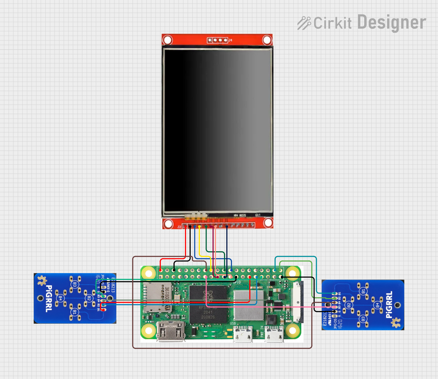
Explore Projects Built with PCB
Common Applications and Use Cases
- Consumer Electronics: Smartphones, laptops, and televisions.
- Industrial Equipment: Control systems, robotics, and automation.
- Medical Devices: Diagnostic equipment and monitoring systems.
- Prototyping: Rapid development of electronic circuits for testing and validation.
- IoT Devices: Smart home systems, wearables, and sensors.
Technical Specifications
Below are the key technical details of the PCB manufactured by Glasgow University:
General Specifications
| Parameter | Value |
|---|---|
| Material | FR4 (Flame Retardant 4) |
| Board Thickness | 1.6 mm |
| Copper Thickness | 1 oz/ft² (35 µm) |
| Layers | Single-layer, Double-layer, or Multi-layer |
| Surface Finish | HASL (Hot Air Solder Leveling) or ENIG (Electroless Nickel Immersion Gold) |
| Solder Mask Color | Green (default), other colors available |
| Operating Temperature | -40°C to 85°C |
| Dielectric Constant (Dk) | 4.2 to 4.7 |
Pin Configuration and Descriptions
While a PCB itself does not have pins, it features pads and vias for connecting components. Below is a table describing common PCB features:
| Feature | Description |
|---|---|
| Pads | Flat conductive areas where components are soldered. |
| Vias | Holes plated with copper to connect layers in multi-layer PCBs. |
| Traces | Conductive pathways that connect components on the PCB. |
| Ground Plane | A large area of copper used as a common ground reference for the circuit. |
| Mounting Holes | Non-conductive holes for securing the PCB to an enclosure or chassis. |
Usage Instructions
How to Use the PCB in a Circuit
- Design the Circuit: Use PCB design software (e.g., KiCad, Eagle, or Altium Designer) to create a schematic and layout.
- Fabricate the PCB: Send the design files (Gerber files) to a PCB manufacturer, such as Glasgow University.
- Assemble Components: Solder components onto the PCB using a soldering iron or reflow soldering process.
- Test the Circuit: Verify the functionality of the assembled PCB using appropriate testing equipment.
Important Considerations and Best Practices
- Trace Width and Spacing: Ensure traces are wide enough to handle the required current and spaced to prevent short circuits.
- Thermal Management: Use thermal vias and heat sinks for components that generate significant heat.
- Grounding: Design a proper ground plane to minimize noise and improve signal integrity.
- Component Placement: Place components logically to minimize trace lengths and avoid interference.
- Inspection: Inspect solder joints and connections for defects before powering the circuit.
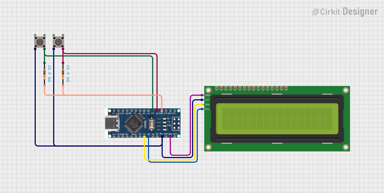
Example: Connecting a PCB to an Arduino UNO
If your PCB is designed to interface with an Arduino UNO, ensure the pin headers on the PCB align with the Arduino's GPIO pins. Below is an example Arduino code snippet for controlling an LED connected to a PCB:
// Example Arduino code to control an LED on a PCB
// Connect the LED to pin 13 on the PCB, which is linked to Arduino's digital pin 13.

void setup() {
  pinMode(13, OUTPUT); // Set pin 13 as an output pin
}

void loop() {
  digitalWrite(13, HIGH); // Turn the LED on
  delay(1000);            // Wait for 1 second
  digitalWrite(13, LOW);  // Turn the LED off
  delay(1000);            // Wait for 1 second
}
Troubleshooting and FAQs
Common Issues Users Might Face
- Short Circuits: Caused by solder bridges or improper trace spacing.
- Solution: Inspect the PCB under a magnifying glass and remove excess solder with a solder wick.
- Open Circuits: Broken traces or poor solder joints.
- Solution: Use a multimeter to check continuity and repair with solder or jumper wires.
- Overheating Components: Caused by insufficient thermal management.
- Solution: Add heat sinks or improve ventilation around the PCB.
- Signal Noise: Poor grounding or trace layout.
- Solution: Redesign the PCB with a proper ground plane and shorter signal traces.
FAQs
Q: Can I use this PCB for high-frequency circuits?
A: Yes, but ensure the PCB design includes impedance-controlled traces and proper grounding to minimize signal loss.
Q: What is the maximum current the PCB can handle?
A: This depends on the trace width and copper thickness. Use a PCB trace width calculator to determine the maximum current capacity.
Q: Can I order custom PCBs from Glasgow University?
A: Yes, Glasgow University offers custom PCB fabrication services. Contact their manufacturing department for details.
Q: How do I clean a PCB after soldering?
A: Use isopropyl alcohol and a soft brush to remove flux residue and other contaminants.
By following this documentation, users can effectively design, assemble, and troubleshoot PCBs for a wide range of applications.