How to Use SN74HC00_FIAX: Examples, Pinouts, and Specs
Introduction
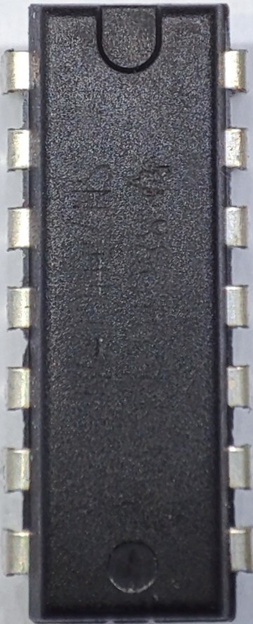
The SN74HC00_FIAX is a quad 2-input NAND gate integrated circuit (IC) from the 74HC00 series, renowned for its high-speed CMOS logic. This versatile component is designed to perform NAND logic operations and is widely used in various digital circuits. Its ability to operate over a wide voltage range makes it suitable for numerous applications, including:
- Digital logic circuits
- Signal processing
- Data manipulation
- Control systems
- Timing and sequencing circuits
Explore Projects Built with SN74HC00_FIAX
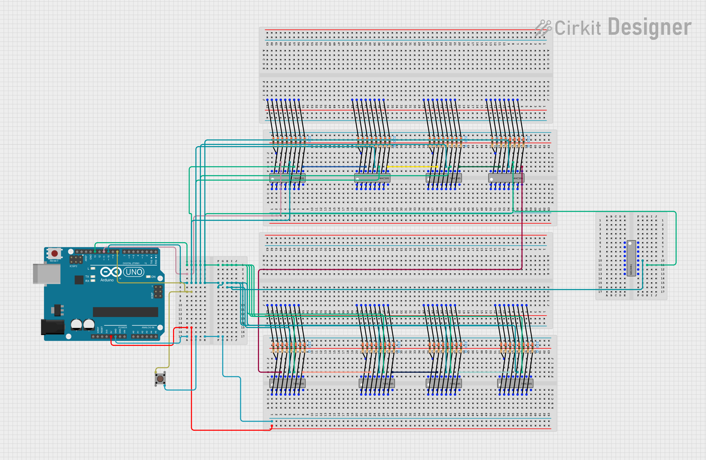
Explore Projects Built with SN74HC00_FIAX
Technical Specifications
Key Technical Details
| Parameter | Value |
|---|---|
| Supply Voltage | 2V to 6V |
| Input Voltage | 0V to Vcc |
| Output Voltage | 0V to Vcc |
| High-Level Input | 2V (min) |
| Low-Level Input | 0.8V (max) |
| High-Level Output | Vcc - 0.1V (min) |
| Low-Level Output | 0.1V (max) |
| Input Current | ±1µA |
| Output Current | ±25mA |
| Power Dissipation | 500mW |
| Propagation Delay | 8ns (typical) |
| Operating Temp. | -40°C to 85°C |
Pin Configuration and Descriptions
| Pin No. | Pin Name | Description |
|---|---|---|
| 1 | 1A | Input A for NAND Gate 1 |
| 2 | 1B | Input B for NAND Gate 1 |
| 3 | 1Y | Output Y for NAND Gate 1 |
| 4 | 2A | Input A for NAND Gate 2 |
| 5 | 2B | Input B for NAND Gate 2 |
| 6 | 2Y | Output Y for NAND Gate 2 |
| 7 | GND | Ground |
| 8 | 3A | Input A for NAND Gate 3 |
| 9 | 3B | Input B for NAND Gate 3 |
| 10 | 3Y | Output Y for NAND Gate 3 |
| 11 | 4A | Input A for NAND Gate 4 |
| 12 | 4B | Input B for NAND Gate 4 |
| 13 | 4Y | Output Y for NAND Gate 4 |
| 14 | Vcc | Supply Voltage |
Usage Instructions
How to Use the Component in a Circuit
- Power Supply: Connect the Vcc pin (Pin 14) to a positive voltage supply (2V to 6V) and the GND pin (Pin 7) to the ground of the circuit.
- Inputs: Connect the input pins (1A, 1B, 2A, 2B, 3A, 3B, 4A, 4B) to the desired logic signals.
- Outputs: The output pins (1Y, 2Y, 3Y, 4Y) will provide the NAND logic result of the corresponding input pairs.
Important Considerations and Best Practices
- Ensure that the supply voltage (Vcc) is within the specified range (2V to 6V).
- Avoid exceeding the maximum input and output current ratings to prevent damage.
- Use decoupling capacitors (e.g., 0.1µF) near the Vcc pin to filter out noise and stabilize the power supply.
- Keep the input signals within the specified voltage range to ensure proper logic operation.
Example Circuit with Arduino UNO
Here is an example of how to use the SN74HC00_FIAX with an Arduino UNO to perform a simple NAND gate operation:
// Define input and output pins
const int inputA = 2;
const int inputB = 3;
const int outputY = 4;

void setup() {
  // Initialize input pins
  pinMode(inputA, INPUT);
  pinMode(inputB, INPUT);

  // Initialize output pin
  pinMode(outputY, OUTPUT);
}

void loop() {
  // Read input values
  int valA = digitalRead(inputA);
  int valB = digitalRead(inputB);

  // Perform NAND operation
  int resultY = !(valA && valB);

  // Output the result
  digitalWrite(outputY, resultY);

  // Small delay for stability
  delay(10);
}
Troubleshooting and FAQs
Common Issues Users Might Face
No Output Signal:
- Solution: Check the power supply connections (Vcc and GND). Ensure that the input signals are within the specified voltage range.
Incorrect Logic Output:
- Solution: Verify the input connections and ensure that the input signals are correctly applied. Check for any loose or faulty connections.
Overheating:
- Solution: Ensure that the current through the IC does not exceed the maximum ratings. Use appropriate heat dissipation methods if necessary.
FAQs
Q1: Can the SN74HC00_FIAX be used with a 3.3V power supply?
- A1: Yes, the SN74HC00_FIAX can operate with a supply voltage range of 2V to 6V, making it compatible with a 3.3V power supply.
Q2: What is the maximum propagation delay of the SN74HC00_FIAX?
- A2: The typical propagation delay is 8ns, but it can vary depending on the operating conditions.
Q3: How many NAND gates are included in the SN74HC00_FIAX?
- A3: The SN74HC00_FIAX contains four independent 2-input NAND gates.
Q4: Can I use the SN74HC00_FIAX for high-speed applications?
- A4: Yes, the SN74HC00_FIAX is designed for high-speed CMOS logic operations, making it suitable for high-speed applications.
By following this documentation, users can effectively integrate the SN74HC00_FIAX into their digital circuits and troubleshoot common issues. Whether you are a beginner or an experienced user, this guide provides the necessary information to utilize this versatile NAND gate IC.