
How to Use Chip antenna: Examples, Pinouts, and Specs
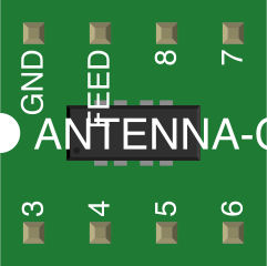
 Design with Chip antenna in Cirkit Designer
Introduction
A chip antenna is a compact antenna designed for wireless communication, commonly used in devices such as smartphones, IoT devices, and other compact electronic systems. It provides efficient signal reception and transmission while maintaining a small form factor, making it ideal for space-constrained applications. Chip antennas are typically used in applications requiring Bluetooth, Wi-Fi, GPS, Zigbee, or other RF communication protocols.
Explore Projects Built with Chip antenna
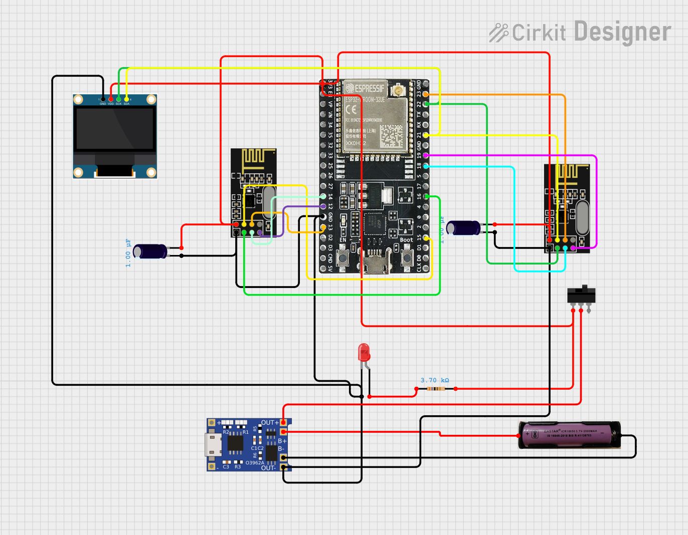 Open Project in Cirkit Designer
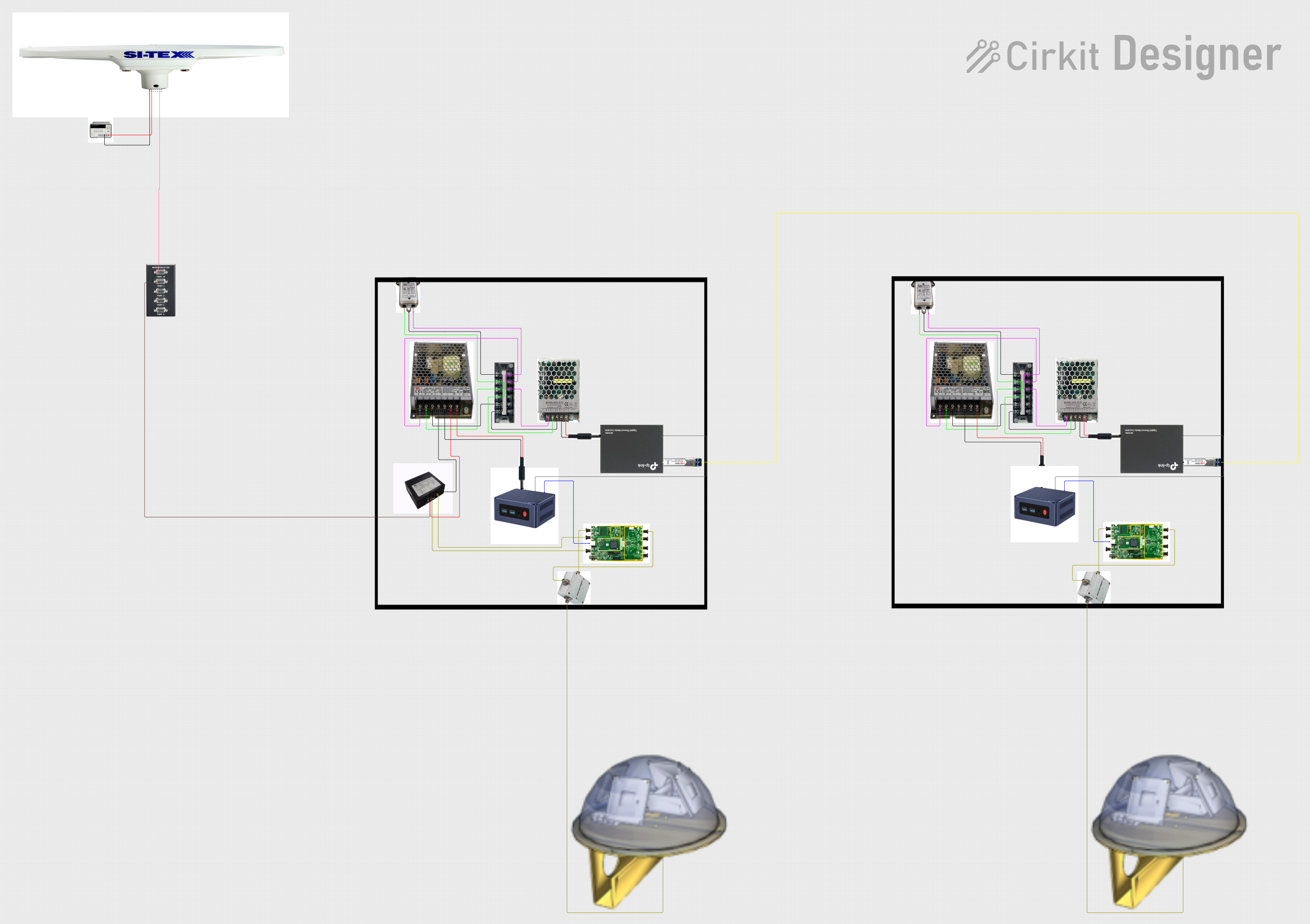 Open Project in Cirkit Designer
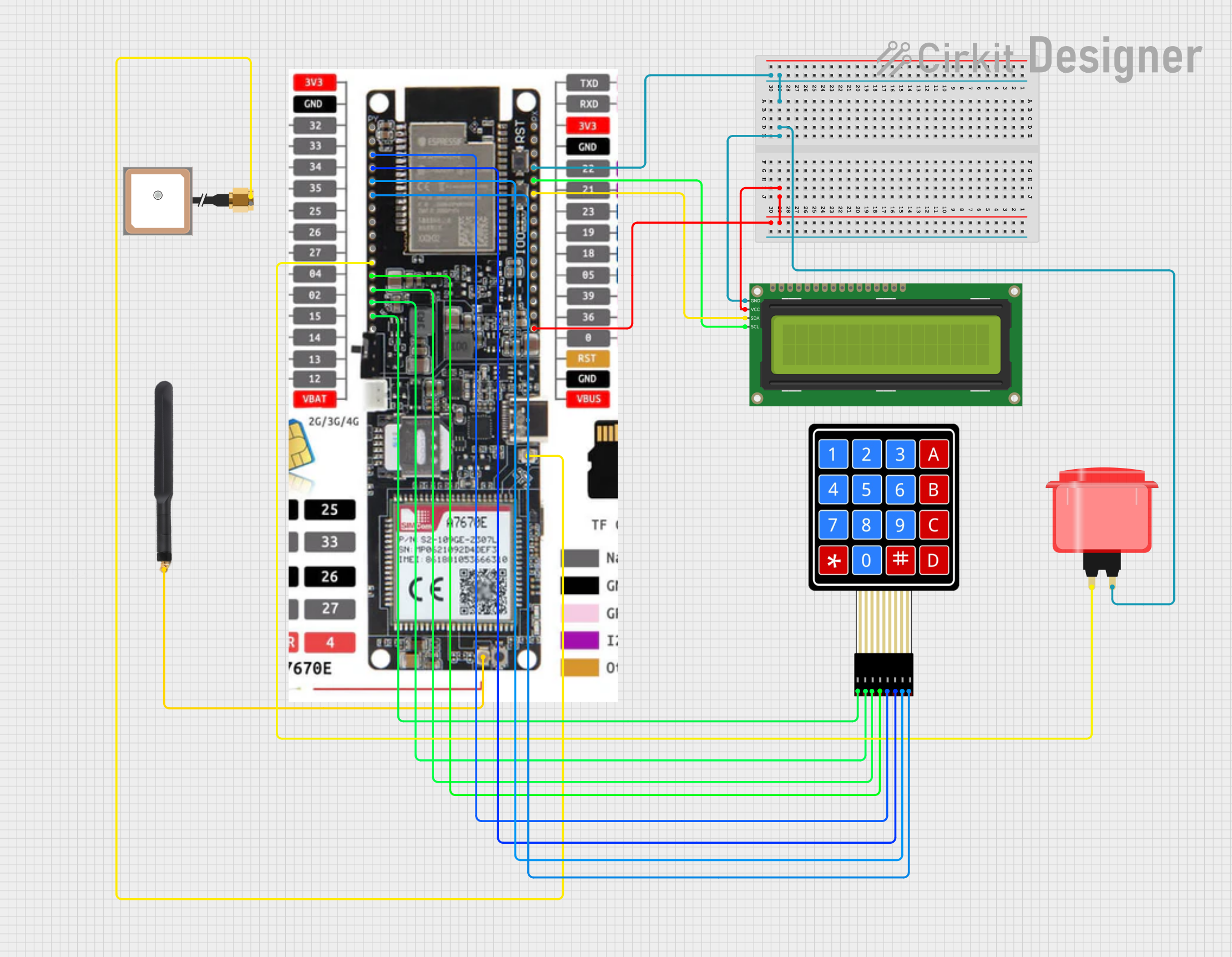 Open Project in Cirkit Designer
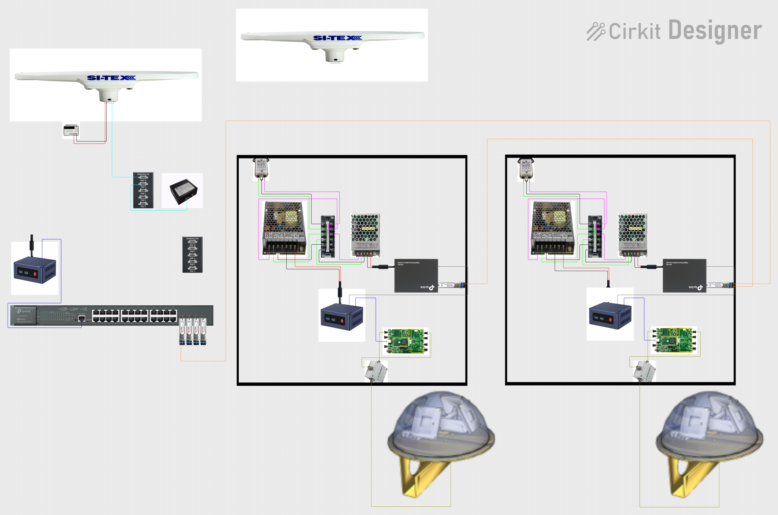 Open Project in Cirkit Designer
Explore Projects Built with Chip antenna
Open Project in Cirkit DesignerOpen Project in Cirkit DesignerOpen Project in Cirkit DesignerOpen Project in Cirkit DesignerCommon Applications:
- Smartphones and tablets
- IoT devices and wearables
- Wireless communication modules (e.g., Wi-Fi, Bluetooth, Zigbee)
- GPS receivers
- Remote controls and key fobs
Technical Specifications
Below are the general technical specifications for a typical chip antenna. Note that specific values may vary depending on the manufacturer and model.
| Parameter | Specification |
|---|---|
| Frequency Range | 2.4 GHz (common for Wi-Fi/Bluetooth) |
| Impedance | 50 Ω |
| Gain | 0 dBi to 3 dBi |
| Polarization | Linear |
| Operating Temperature | -40°C to +85°C |
| Dimensions | 1 mm x 2 mm x 0.5 mm (varies by model) |
| VSWR (Voltage Standing Wave Ratio) | ≤ 2.0 |
Pin Configuration and Descriptions
Chip antennas typically do not have traditional pins like ICs. Instead, they are surface-mounted components with solder pads. Below is a general description of the connections:
| Pad Name | Description |
|---|---|
| RF Input | Connects to the RF signal source (e.g., RF module) |
| Ground (GND) | Connects to the ground plane of the PCB |
Usage Instructions
How to Use a Chip Antenna in a Circuit
Placement on PCB:
- Place the chip antenna on the PCB in a location with minimal interference from other components.
- Ensure the antenna is positioned near the edge of the PCB for optimal performance.
Ground Plane Design:
- Provide a clear ground plane under the antenna for proper impedance matching.
- Avoid placing any traces or components directly beneath the antenna.
Matching Network:
- Use an impedance matching network (e.g., capacitors and inductors) between the RF source and the antenna to ensure a 50 Ω impedance match.
- Refer to the antenna's datasheet for recommended matching network values.
Soldering:
- Use proper soldering techniques to attach the chip antenna to the PCB.
- Avoid excessive heat to prevent damage to the component.
Testing:
- Use an RF analyzer or network analyzer to verify the antenna's performance.
- Check for proper VSWR and signal strength.
Important Considerations and Best Practices
- Keep Clearances: Maintain a clear area around the antenna to avoid signal degradation.
- Avoid Metal Enclosures: Metal enclosures can block or reflect RF signals, reducing performance.
- Use Proper Tools: Use an RF analyzer to fine-tune the matching network for optimal performance.
- Follow Manufacturer Guidelines: Always refer to the specific chip antenna's datasheet for detailed recommendations.
Example: Using a Chip Antenna with an Arduino UNO
Below is an example of connecting a chip antenna to a Bluetooth module, which is then interfaced with an Arduino UNO.
Circuit Diagram
- Connect the chip antenna to the RF input of the Bluetooth module.
- Connect the Bluetooth module's TX, RX, VCC, and GND pins to the Arduino UNO as follows:
- TX → Arduino RX (Pin 0)
- RX → Arduino TX (Pin 1)
- VCC → Arduino 5V
- GND → Arduino GND
Arduino Code Example
#include <SoftwareSerial.h>

// Define RX and TX pins for Bluetooth communication
SoftwareSerial bluetooth(10, 11); // RX = Pin 10, TX = Pin 11

void setup() {
  Serial.begin(9600); // Initialize Serial Monitor
  bluetooth.begin(9600); // Initialize Bluetooth module

  Serial.println("Bluetooth Chip Antenna Example");
  bluetooth.println("Hello from Arduino!");
}

void loop() {
  // Check if data is received from Bluetooth
  if (bluetooth.available()) {
    char data = bluetooth.read(); // Read data from Bluetooth
    Serial.print("Received: ");
    Serial.println(data); // Print data to Serial Monitor
  }

  // Check if data is sent from Serial Monitor
  if (Serial.available()) {
    char data = Serial.read(); // Read data from Serial Monitor
    bluetooth.print(data); // Send data to Bluetooth
  }
}
Troubleshooting and FAQs
Common Issues
Weak Signal Strength:
- Cause: Poor placement of the antenna or interference from nearby components.
- Solution: Reposition the antenna closer to the PCB edge and ensure a clear area around it.
High VSWR:
- Cause: Impedance mismatch between the RF source and the antenna.
- Solution: Adjust the matching network components to achieve a 50 Ω impedance match.
No Signal Reception:
- Cause: Incorrect soldering or damaged antenna.
- Solution: Inspect solder joints and replace the antenna if necessary.
Interference from Metal Enclosures:
- Cause: Metal casing blocking RF signals.
- Solution: Use a plastic or non-metallic enclosure, or position the antenna outside the metal casing.
FAQs
Q1: Can I use a chip antenna for multiple frequency bands?
A1: Some chip antennas are designed for multiple frequency bands (e.g., dual-band Wi-Fi). Check the datasheet to confirm compatibility.
Q2: Do I need a matching network for every chip antenna?
A2: Yes, most chip antennas require a matching network to ensure proper impedance matching and optimal performance.
Q3: How do I test the performance of a chip antenna?
A3: Use an RF analyzer or network analyzer to measure parameters like VSWR, gain, and signal strength.
Q4: Can I use a chip antenna in a high-temperature environment?
A4: Most chip antennas operate within -40°C to +85°C. Check the specific model's datasheet for exact temperature ratings.