How to Use T74LS10B1/T54LS10_FIAX: Examples, Pinouts, and Specs
Introduction
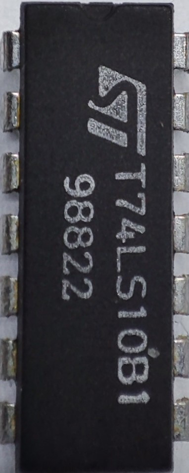
The T74LS10B1/T54LS10_FIAX is a triple 3-input NAND gate integrated circuit (IC) from the 74LS series. This series is renowned for its low power consumption and high-speed performance. The T74LS10B1/T54LS10_FIAX is widely used in digital circuits to perform logical NAND operations, making it a fundamental component in various electronic applications.
Explore Projects Built with T74LS10B1/T54LS10_FIAX
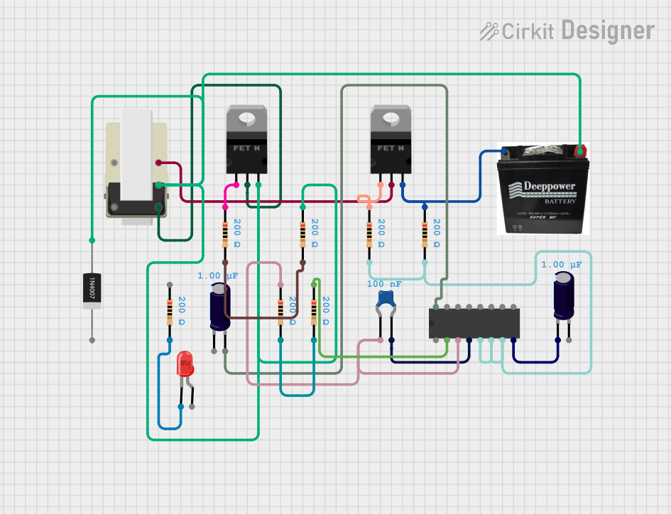
Explore Projects Built with T74LS10B1/T54LS10_FIAX
Common Applications and Use Cases
- Digital Logic Circuits: Used for creating complex logic functions.
- Microcontroller Interfacing: Commonly used with microcontrollers like Arduino for logical operations.
- Signal Processing: Employed in signal processing circuits for combining multiple signals.
- Control Systems: Utilized in control systems for decision-making processes.
Technical Specifications
Key Technical Details
| Parameter | Value |
|---|---|
| Supply Voltage | 4.75V to 5.25V |
| Input Voltage | 0V to 5.5V |
| High-Level Output | 2.7V (min) |
| Low-Level Output | 0.5V (max) |
| High-Level Input | 2V (min) |
| Low-Level Input | 0.8V (max) |
| Propagation Delay | 9ns (typical) |
| Power Dissipation | 20mW (typical) |
| Operating Temperature | -55°C to 125°C |
Pin Configuration and Descriptions
| Pin No. | Pin Name | Description |
|---|---|---|
| 1 | 1A | Input A for Gate 1 |
| 2 | 1B | Input B for Gate 1 |
| 3 | 1C | Input C for Gate 1 |
| 4 | 1Y | Output for Gate 1 |
| 5 | 2A | Input A for Gate 2 |
| 6 | 2B | Input B for Gate 2 |
| 7 | 2C | Input C for Gate 2 |
| 8 | 2Y | Output for Gate 2 |
| 9 | GND | Ground |
| 10 | 3A | Input A for Gate 3 |
| 11 | 3B | Input B for Gate 3 |
| 12 | 3C | Input C for Gate 3 |
| 13 | 3Y | Output for Gate 3 |
| 14 | VCC | Supply Voltage |
Usage Instructions
How to Use the Component in a Circuit
- Power Supply: Connect pin 14 (VCC) to a 5V power supply and pin 9 (GND) to ground.
- Inputs: Connect the inputs (1A, 1B, 1C, etc.) to the desired logic signals.
- Outputs: The outputs (1Y, 2Y, 3Y) will provide the NAND operation results.
Important Considerations and Best Practices
- Decoupling Capacitors: Place a 0.1µF decoupling capacitor close to the VCC pin to filter out noise.
- Unused Inputs: Tie unused inputs to either VCC or GND to prevent floating inputs, which can cause unpredictable behavior.
- Input Voltage Levels: Ensure that input voltage levels are within the specified range to avoid damage to the IC.
Example Circuit with Arduino UNO
// Example code to demonstrate the use of T74LS10B1/T54LS10_FIAX with Arduino UNO

const int inputA = 2; // Input A connected to digital pin 2
const int inputB = 3; // Input B connected to digital pin 3
const int inputC = 4; // Input C connected to digital pin 4
const int outputY = 5; // Output Y connected to digital pin 5

void setup() {
  pinMode(inputA, OUTPUT);
  pinMode(inputB, OUTPUT);
  pinMode(inputC, OUTPUT);
  pinMode(outputY, INPUT);
  Serial.begin(9600);
}

void loop() {
  digitalWrite(inputA, HIGH); // Set input A to HIGH
  digitalWrite(inputB, HIGH); // Set input B to HIGH
  digitalWrite(inputC, LOW);  // Set input C to LOW

  int outputValue = digitalRead(outputY); // Read the output value
  Serial.print("Output Y: ");
  Serial.println(outputValue); // Print the output value to the serial monitor

  delay(1000); // Wait for 1 second
}
Troubleshooting and FAQs
Common Issues Users Might Face
No Output Signal:
- Solution: Check the power supply connections (VCC and GND). Ensure that the input signals are within the specified voltage range.
Unstable Output:
- Solution: Use decoupling capacitors to filter out noise. Ensure that all unused inputs are tied to VCC or GND.
Incorrect Logic Operation:
- Solution: Verify the input connections and ensure that the logic levels are correctly set.
FAQs
Q1: Can I use the T74LS10B1/T54LS10_FIAX with a 3.3V power supply?
- A1: No, the T74LS10B1/T54LS10_FIAX is designed to operate with a 5V power supply. Using a 3.3V supply may result in incorrect operation or damage to the IC.
Q2: How do I connect multiple NAND gates in a circuit?
- A2: You can connect the outputs of one NAND gate to the inputs of another to create more complex logic functions. Ensure that the input and output voltage levels are compatible.
Q3: What is the maximum operating temperature for the T74LS10B1/T54LS10_FIAX?
- A3: The maximum operating temperature is 125°C. Ensure that the IC is used within this temperature range to avoid damage.
This documentation provides a comprehensive overview of the T74LS10B1/T54LS10_FIAX triple 3-input NAND gate IC, including its technical specifications, usage instructions, and troubleshooting tips. Whether you are a beginner or an experienced user, this guide will help you effectively utilize this component in your electronic projects.