How to Use ADC0804: Examples, Pinouts, and Specs
Introduction
The ADC0804 is an 8-bit analog-to-digital converter (ADC) manufactured by Texas Instruments, with the part ID ADC0804LCN. This component is designed to convert analog signals into digital data, making it an essential tool in data acquisition and processing systems. It operates with a single power supply and supports input voltages ranging from 0 to 5V. The ADC0804 features a parallel output for fast data transfer and is widely used in applications requiring precise analog-to-digital conversion.
Explore Projects Built with ADC0804
Explore Projects Built with ADC0804
Common Applications and Use Cases
- Data acquisition systems
- Microcontroller-based projects
- Signal processing
- Industrial automation
- Sensor interfacing (e.g., temperature, pressure, or light sensors)
Technical Specifications
The ADC0804 is a versatile and reliable ADC with the following key specifications:
| Parameter | Value |
|---|---|
| Resolution | 8 bits |
| Input Voltage Range | 0V to 5V |
| Reference Voltage (Vref) | Adjustable (up to 5V) |
| Conversion Time | 100 µs (typical) |
| Supply Voltage (Vcc) | 4.5V to 6V |
| Input Current | ±1 µA (typical) |
| Output Format | Parallel (8-bit) |
| Operating Temperature | 0°C to 70°C |
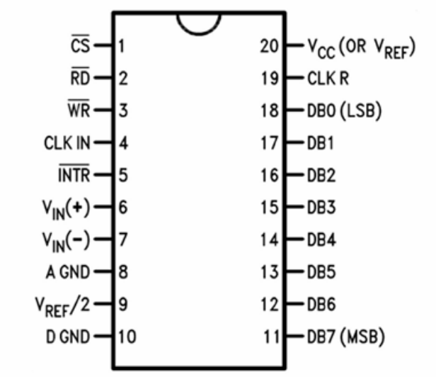
Pin Configuration and Descriptions
The ADC0804 comes in a 20-pin Dual Inline Package (DIP). Below is the pinout and description:
| Pin Number | Pin Name | Description |
|---|---|---|
| 1 | CS | Chip Select (active low). Enables the ADC when pulled low. |
| 2 | RD | Read (active low). Outputs the converted data when pulled low. |
| 3 | WR | Write (active low). Starts the conversion process when pulled low. |
| 4 | CLK IN | External clock input. |
| 5 | INTR | Interrupt output. Goes low when conversion is complete. |
| 6 | Vref/2 | Reference voltage input. Sets the analog input range. |
| 7 | AGND | Analog ground. |
| 8 | Vin(+) | Analog input signal. |
| 9 | Vin(-) | Analog input ground (typically connected to AGND). |
| 10 | DGND | Digital ground. |
| 11–18 | D0–D7 | Digital output pins (8-bit parallel data). |
| 19 | Vcc | Power supply (4.5V to 6V). |
| 20 | CLK R | Clock resistor input. Used to generate an internal clock with an external resistor. |
Usage Instructions
How to Use the ADC0804 in a Circuit
Power Supply and Grounding:
- Connect
Vccto a 5V power supply. - Connect
AGNDandDGNDto the ground of the circuit.
- Connect
Reference Voltage:
- Connect a reference voltage to the
Vref/2pin. For a full-scale input range of 0–5V, connectVref/2to 2.5V.
- Connect a reference voltage to the
Clock Signal:
- Provide a clock signal to the
CLK INpin. This can be done using an external oscillator or by connecting a resistor to theCLK Rpin for an internal clock.
- Provide a clock signal to the
Analog Input:
- Connect the analog signal to be converted to the
Vin(+)pin. Ensure the signal is within the 0–5V range.
- Connect the analog signal to be converted to the
Start Conversion:
- Pull the
WRpin low to start the conversion process.
- Pull the
Read Data:
- Wait for the
INTRpin to go low, indicating the conversion is complete. - Pull the
RDpin low to read the 8-bit digital output from theD0–D7pins.
- Wait for the
Important Considerations and Best Practices
- Ensure the analog input signal does not exceed the reference voltage to avoid inaccurate conversions.
- Use decoupling capacitors (e.g., 0.1 µF) near the power supply pins to reduce noise.
- If using the internal clock, select an appropriate resistor value for the
CLK Rpin to achieve the desired clock frequency. - Avoid leaving unused pins floating; connect them to ground or a defined logic level.
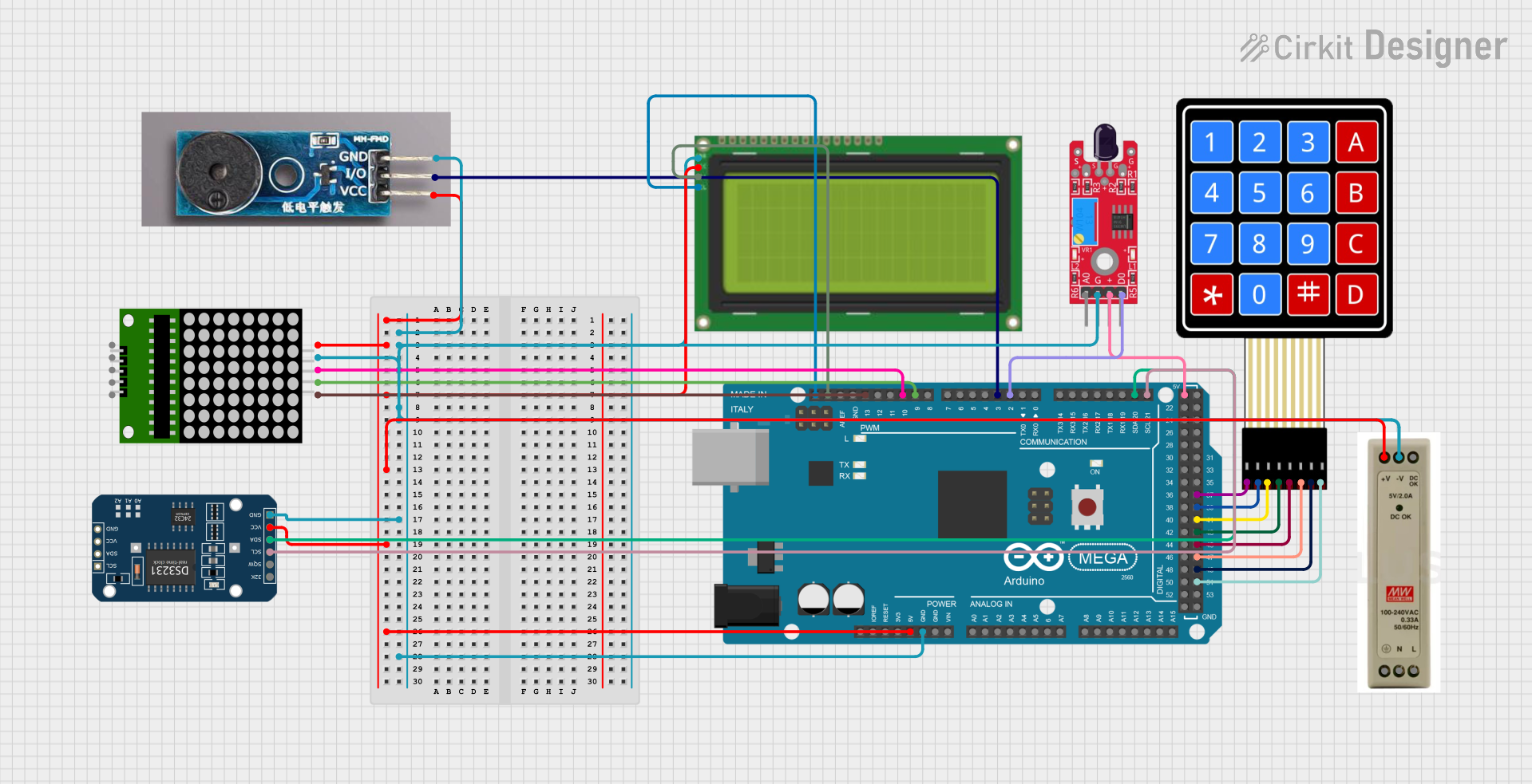
Example: Interfacing ADC0804 with Arduino UNO
Below is an example of how to interface the ADC0804 with an Arduino UNO to read an analog signal and display the digital output.
Circuit Connections
- Connect
Vccto the Arduino's 5V pin andAGND/DGNDto the Arduino's GND. - Connect the
Vin(+)pin to the analog signal source. - Connect the
D0–D7pins to Arduino digital pins 2–9. - Connect
CS,RD, andWRto Arduino digital pins 10, 11, and 12, respectively. - Connect
INTRto Arduino digital pin 13.
Arduino Code
// Define ADC0804 pins
#define CS 10    // Chip Select
#define RD 11    // Read
#define WR 12    // Write
#define INTR 13  // Interrupt
#define D0 2     // Digital output pins D0–D7
#define D7 9

void setup() {
  // Configure control pins as outputs
  pinMode(CS, OUTPUT);
  pinMode(RD, OUTPUT);
  pinMode(WR, OUTPUT);
  pinMode(INTR, INPUT);

  // Configure data pins as inputs
  for (int i = D0; i <= D7; i++) {
    pinMode(i, INPUT);
  }

  // Initialize control pins
  digitalWrite(CS, HIGH);
  digitalWrite(RD, HIGH);
  digitalWrite(WR, HIGH);

  Serial.begin(9600); // Start serial communication
}

void loop() {
  // Start conversion
  digitalWrite(CS, LOW);
  digitalWrite(WR, LOW);
  delayMicroseconds(1); // Small delay for write pulse
  digitalWrite(WR, HIGH);

  // Wait for conversion to complete
  while (digitalRead(INTR) == HIGH);

  // Read digital output
  digitalWrite(RD, LOW);
  int digitalValue = 0;
  for (int i = D0; i <= D7; i++) {
    digitalValue |= (digitalRead(i) << (i - D0));
  }
  digitalWrite(RD, HIGH);

  // Print the digital value
  Serial.println(digitalValue);

  delay(500); // Delay for readability
}
Troubleshooting and FAQs
Common Issues and Solutions
No Output or Incorrect Data:
- Verify the power supply connections (
Vcc,AGND, andDGND). - Ensure the analog input signal is within the 0–5V range.
- Check the reference voltage (
Vref/2) and ensure it is correctly set.
- Verify the power supply connections (
Conversion Not Completing:
- Confirm that the clock signal is present and within the required frequency range.
- Check the
WRandCSsignals to ensure the conversion process is being triggered.
Noise in Output:
- Use decoupling capacitors near the power supply pins.
- Shield the analog input signal from external noise sources.
FAQs
Q: Can the ADC0804 handle negative input voltages?
A: No, the ADC0804 is designed for unipolar input signals (0–5V). Negative voltages may damage the component.
Q: What is the purpose of the Vref/2 pin?
A: The Vref/2 pin sets the reference voltage for the ADC, determining the full-scale input range. For a 0–5V range, connect Vref/2 to 2.5V.
Q: Can I use the ADC0804 without an external clock?
A: Yes, you can use the internal clock by connecting a resistor to the CLK R pin. Select an appropriate resistor value to achieve the desired clock frequency.