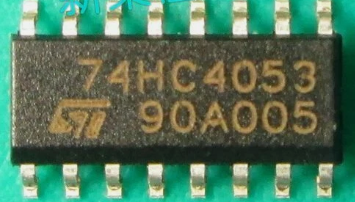
How to Use 74HC4053: Examples, Pinouts, and Specs
Introduction
The 74HC4053 is a triple 2-channel analog multiplexer/demultiplexer with independent enable inputs. It is a versatile quad bilateral switch that can control analog signals, allowing both positive and negative voltages to pass through. The component is designed with low on-resistance, making it ideal for applications requiring minimal signal distortion.
Explore Projects Built with 74HC4053
Explore Projects Built with 74HC4053
Common Applications:
- Audio signal routing
- Analog multiplexing and demultiplexing
- Signal gating and switching
- Data acquisition systems
- Sensor signal selection
Technical Specifications
The 74HC4053 operates as a triple 2-channel switch, where each switch can independently connect one of two inputs to a common output. Below are the key technical details:
Key Specifications:
- Supply Voltage (Vcc): 2V to 6V
- Control Input Voltage Range: 0V to Vcc
- Analog Signal Range: -6V to +6V (with Vcc = 6V)
- On-Resistance (Ron): ~70Ω (typical at Vcc = 4.5V)
- Propagation Delay: ~10ns (typical at Vcc = 5V)
- Maximum Switching Frequency: 6 MHz
- Operating Temperature Range: -40°C to +85°C
- Package Types: DIP-16, SOIC-16, TSSOP-16
Pin Configuration and Descriptions:
The 74HC4053 comes in a 16-pin package. Below is the pinout and description:
| Pin Number | Pin Name | Description |
|---|---|---|
| 1 | VEE | Negative supply voltage (connect to GND for single-supply operation) |
| 2 | C1 | Control input for switch 1 |
| 3 | B1 | Control input for switch 2 |
| 4 | A1 | Control input for switch 3 |
| 5 | IN1A | Input A for switch 1 |
| 6 | IN1B | Input B for switch 1 |
| 7 | OUT1 | Common output for switch 1 |
| 8 | GND | Ground |
| 9 | OUT2 | Common output for switch 2 |
| 10 | IN2B | Input B for switch 2 |
| 11 | IN2A | Input A for switch 2 |
| 12 | OUT3 | Common output for switch 3 |
| 13 | IN3B | Input B for switch 3 |
| 14 | IN3A | Input A for switch 3 |
| 15 | VCC | Positive supply voltage |
| 16 | ENABLE | Enable pin (active LOW) |
Usage Instructions
The 74HC4053 is straightforward to use in analog switching and multiplexing applications. Below are the steps and considerations for using the component:
Basic Circuit Connection:
Power Supply:
- Connect the VCC pin to a positive voltage source (e.g., 5V).
- Connect the VEE pin to GND for single-supply operation or to a negative voltage for dual-supply operation.
- Connect the GND pin to the circuit ground.
Control Inputs:
- Use the A1, B1, and C1 pins to control the switches. A HIGH or LOW signal on these pins determines which input (A or B) is connected to the output.
Enable Pin:
- The ENABLE pin must be set LOW to activate the switches. If set HIGH, all switches are disabled.
Signal Connections:
- Connect the analog signals to the INxA and INxB pins.
- The selected signal will appear on the corresponding OUTx pin.
Example Circuit:
Below is an example of using the 74HC4053 to switch between two audio signals:
/*
 * Example: Controlling the 74HC4053 with an Arduino UNO
 * This code demonstrates how to toggle between two analog signals
 * using the control pins of the 74HC4053.
 */

const int controlPinA = 2; // Connect to A1 pin of 74HC4053
const int controlPinB = 3; // Connect to B1 pin of 74HC4053
const int enablePin = 4;   // Connect to ENABLE pin of 74HC4053

void setup() {
  pinMode(controlPinA, OUTPUT); // Set control pin A as output
  pinMode(controlPinB, OUTPUT); // Set control pin B as output
  pinMode(enablePin, OUTPUT);   // Set enable pin as output

  digitalWrite(enablePin, LOW); // Enable the 74HC4053
}

void loop() {
  // Switch to Input A
  digitalWrite(controlPinA, LOW);
  digitalWrite(controlPinB, LOW);
  delay(1000); // Wait for 1 second

  // Switch to Input B
  digitalWrite(controlPinA, HIGH);
  digitalWrite(controlPinB, LOW);
  delay(1000); // Wait for 1 second
}
Important Considerations:
- Ensure the analog signal voltage does not exceed the supply voltage range.
- For dual-supply operation, connect VEE to a negative voltage (e.g., -5V) to handle negative analog signals.
- Use decoupling capacitors (e.g., 0.1µF) near the power supply pins to reduce noise.
Troubleshooting and FAQs
Common Issues:
No Signal Output:
- Ensure the ENABLE pin is set LOW.
- Verify the control pins (A1, B1, C1) are receiving the correct logic levels.
Signal Distortion:
- Check if the analog signal voltage exceeds the supply voltage range.
- Verify the on-resistance (Ron) is acceptable for your application.
Switching Noise:
- Add bypass capacitors near the power supply pins.
- Use proper grounding techniques to minimize noise.
FAQs:
Q1: Can the 74HC4053 handle digital signals?
A1: Yes, the 74HC4053 can switch digital signals as well as analog signals.
Q2: What happens if the ENABLE pin is left floating?
A2: The behavior is undefined. Always connect the ENABLE pin to a defined logic level (HIGH or LOW).
Q3: Can I use the 74HC4053 with a single power supply?
A3: Yes, connect VEE to GND for single-supply operation. However, this limits the analog signal range to 0V to VCC.
By following these guidelines, the 74HC4053 can be effectively used in a variety of analog and digital switching applications.