
How to Use HEF4094: Examples, Pinouts, and Specs
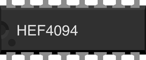
 Design with HEF4094 in Cirkit Designer
Introduction
The HEF4094 is a dual 4-stage static shift register with a serial input and parallel output. It is widely used in digital circuits for data storage and manipulation, enabling the controlled shifting of data bits. This component is particularly useful in applications requiring serial-to-parallel data conversion, LED driving, and cascading multiple shift registers for extended data handling.
Explore Projects Built with HEF4094
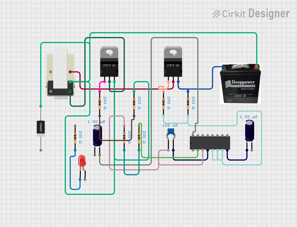 Open Project in Cirkit Designer
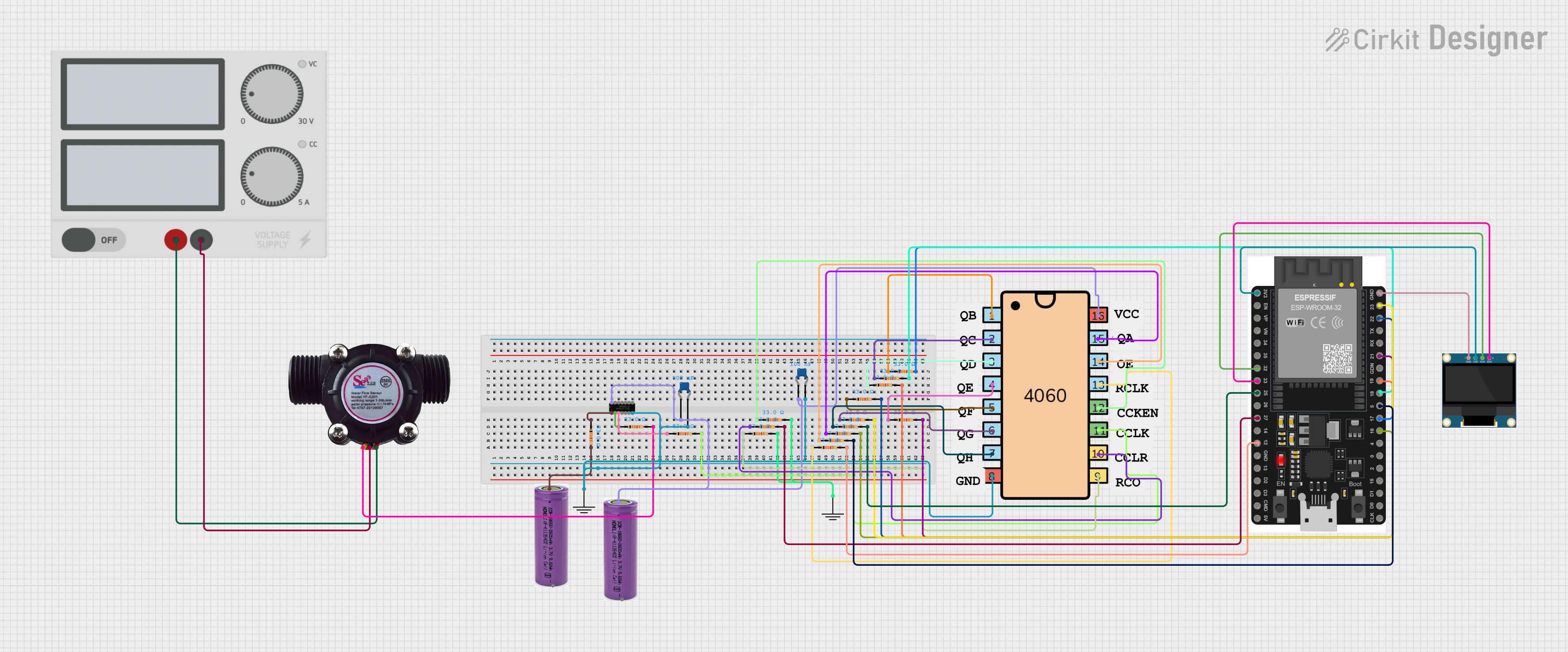 Open Project in Cirkit Designer
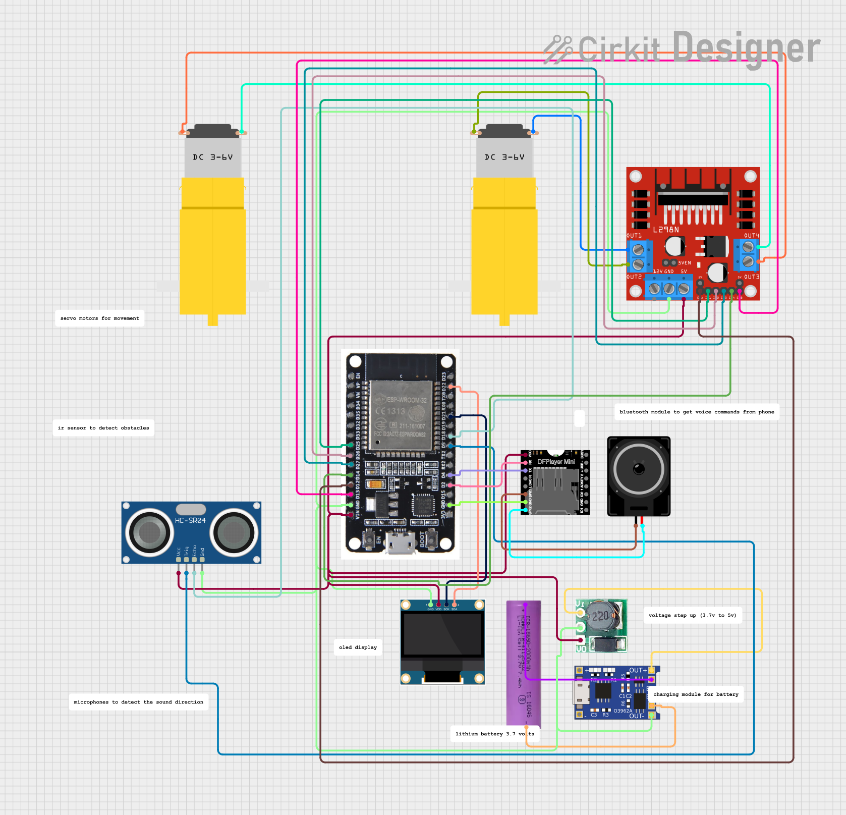 Open Project in Cirkit Designer
 Open Project in Cirkit Designer
Explore Projects Built with HEF4094
Open Project in Cirkit DesignerOpen Project in Cirkit DesignerOpen Project in Cirkit DesignerOpen Project in Cirkit DesignerCommon Applications:
- Serial-to-parallel data conversion
- LED matrix control
- Driving 7-segment displays
- Expanding microcontroller I/O pins
- Cascading for extended shift register chains
Technical Specifications
The HEF4094 is a versatile and reliable shift register with the following key specifications:
| Parameter | Value |
|---|---|
| Supply Voltage (VDD) | 3V to 15V |
| Input Voltage Range | 0V to VDD |
| Maximum Clock Frequency | 8 MHz (at VDD = 15V) |
| Output Current (per pin) | ±10 mA |
| Operating Temperature Range | -40°C to +85°C |
| Package Types | DIP-16, SO-16, TSSOP-16 |
Pin Configuration and Descriptions
The HEF4094 has a 16-pin configuration as shown below:
| Pin Number | Pin Name | Description |
|---|---|---|
| 1 | Q1 | Parallel output of the first stage |
| 2 | Q2 | Parallel output of the second stage |
| 3 | Q3 | Parallel output of the third stage |
| 4 | Q4 | Parallel output of the fourth stage |
| 5 | Q5 | Parallel output of the fifth stage |
| 6 | Q6 | Parallel output of the sixth stage |
| 7 | Q7 | Parallel output of the seventh stage |
| 8 | GND | Ground (0V) |
| 9 | Q8 | Parallel output of the eighth stage |
| 10 | CP (Clock) | Clock input for shifting data |
| 11 | STROBE | Strobe input for latching data to the outputs |
| 12 | DATA | Serial data input |
| 13 | Qs | Serial data output (for cascading multiple HEF4094s) |
| 14 | OE (Output Enable) | Enables or disables the parallel outputs (active LOW) |
| 15 | MR (Master Reset) | Resets all shift register stages to LOW (active LOW) |
| 16 | VDD | Positive supply voltage |
Usage Instructions
How to Use the HEF4094 in a Circuit
- Power Supply: Connect the VDD pin to a voltage source (3V to 15V) and the GND pin to ground.
- Data Input: Feed serial data into the DATA pin. Data is shifted into the register on the rising edge of the clock signal (CP pin).
- Clock Signal: Provide a clock signal to the CP pin to control the shifting of data.
- Strobe Signal: Use the STROBE pin to latch the shifted data into the parallel output pins (Q1 to Q8).
- Output Enable: The OE pin must be held LOW to enable the parallel outputs. If HIGH, the outputs are disabled.
- Reset: Use the MR pin to reset all shift register stages to LOW when needed.
Example Circuit with Arduino UNO
The following example demonstrates how to use the HEF4094 with an Arduino UNO to control 8 LEDs:
Circuit Connections:
- Connect the HEF4094's VDD to 5V and GND to ground.
- Connect the DATA pin to Arduino pin 8.
- Connect the CP (Clock) pin to Arduino pin 9.
- Connect the STROBE pin to Arduino pin 10.
- Connect the OE pin to ground (to enable outputs).
- Connect the Q1 to Q8 pins to the cathodes of 8 LEDs (with current-limiting resistors).
Arduino Code:
// Pin definitions for HEF4094
const int dataPin = 8;    // Serial data input
const int clockPin = 9;   // Clock input
const int strobePin = 10; // Strobe input

void setup() {
  // Set pins as outputs
  pinMode(dataPin, OUTPUT);
  pinMode(clockPin, OUTPUT);
  pinMode(strobePin, OUTPUT);

  // Initialize pins to LOW
  digitalWrite(dataPin, LOW);
  digitalWrite(clockPin, LOW);
  digitalWrite(strobePin, LOW);
}

void loop() {
  // Example: Shift out a binary pattern (e.g., 10101010)
  byte data = 0b10101010;

  // Send data to HEF4094
  shiftOut(dataPin, clockPin, MSBFIRST, data);

  // Latch data to outputs
  digitalWrite(strobePin, HIGH);
  delay(10); // Small delay for stability
  digitalWrite(strobePin, LOW);

  // Wait before sending the next pattern
  delay(1000);
}
Best Practices:
- Use decoupling capacitors (e.g., 0.1 µF) near the VDD pin to stabilize the power supply.
- Avoid exceeding the maximum clock frequency to ensure reliable operation.
- Use pull-down resistors on control pins (e.g., OE, MR) if they are not actively driven.
Troubleshooting and FAQs
Common Issues and Solutions:
No Output on Q1 to Q8 Pins:
- Ensure the OE pin is connected to ground (active LOW).
- Verify that the STROBE pin is toggled after shifting data.
Data Not Shifting Correctly:
- Check the clock signal on the CP pin. Ensure it is a clean square wave.
- Verify the DATA pin connection and ensure the input data is correct.
Outputs Flickering or Unstable:
- Add decoupling capacitors near the VDD pin to reduce noise.
- Ensure the clock frequency does not exceed the maximum rating.
Cascading Multiple HEF4094s Not Working:
- Verify the Qs pin of the first HEF4094 is connected to the DATA pin of the next.
- Ensure all HEF4094s share the same clock and strobe signals.
FAQs:
Q: Can the HEF4094 drive high-power LEDs directly?
A: No, the HEF4094's output current is limited to ±10 mA per pin. Use external transistors or drivers for high-power LEDs.
Q: How many HEF4094s can be cascaded?
A: Theoretically, any number can be cascaded, but practical limitations like signal degradation and timing constraints should be considered.
Q: What happens if the OE pin is left floating?
A: The outputs may behave unpredictably. Always connect the OE pin to a defined logic level (LOW to enable outputs).