How to Use CD4093: Examples, Pinouts, and Specs
Introduction
The CD4093 is a quad 2-input NAND Schmitt trigger IC manufactured by Texas Instruments. It is designed to provide a high degree of noise immunity and is widely used in digital circuits for signal conditioning, waveform shaping, and logic-level conversion. The Schmitt trigger functionality ensures that the output switches cleanly between logic states, even when the input signal is noisy or has slow transitions.
Explore Projects Built with CD4093
Explore Projects Built with CD4093
Common Applications
- Signal conditioning in noisy environments
- Waveform generation and shaping
- Pulse-width modulation (PWM) circuits
- Oscillators and timers
- Logic-level conversion
- Debouncing mechanical switches
Technical Specifications
The following table outlines the key technical specifications of the CD4093:
| Parameter | Value |
|---|---|
| Supply Voltage (VDD) | 3V to 15V |
| Input Voltage Range | 0V to VDD |
| Output Voltage Range | 0V to VDD |
| Maximum Output Current | ±10 mA |
| Quiescent Current (Max) | 20 µA at 5V, 40 µA at 10V |
| Propagation Delay (Typical) | 200 ns at 5V, 100 ns at 10V |
| Operating Temperature Range | -55°C to +125°C |
| Logic Type | CMOS |
| Package Types | PDIP, SOIC, TSSOP, and others |
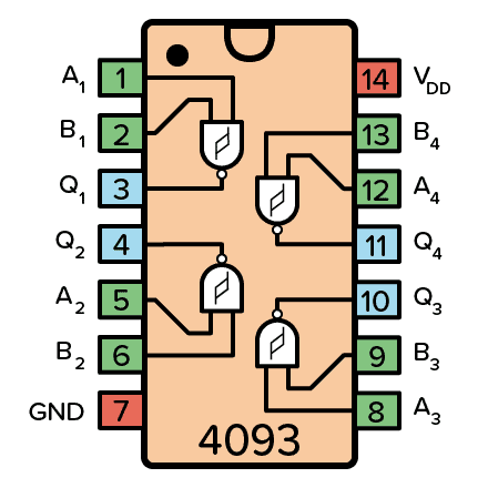
Pin Configuration and Descriptions
The CD4093 has a total of 14 pins. The pinout and their descriptions are as follows:
| Pin Number | Pin Name | Description |
|---|---|---|
| 1 | A1 | Input A for NAND Gate 1 |
| 2 | B1 | Input B for NAND Gate 1 |
| 3 | Q1 | Output of NAND Gate 1 |
| 4 | A2 | Input A for NAND Gate 2 |
| 5 | B2 | Input B for NAND Gate 2 |
| 6 | Q2 | Output of NAND Gate 2 |
| 7 | VSS | Ground (0V) |
| 8 | Q3 | Output of NAND Gate 3 |
| 9 | A3 | Input A for NAND Gate 3 |
| 10 | B3 | Input B for NAND Gate 3 |
| 11 | Q4 | Output of NAND Gate 4 |
| 12 | A4 | Input A for NAND Gate 4 |
| 13 | B4 | Input B for NAND Gate 4 |
| 14 | VDD | Positive Supply Voltage |
Usage Instructions
How to Use the CD4093 in a Circuit
- Power Supply: Connect the VDD pin (Pin 14) to the positive supply voltage (3V to 15V) and the VSS pin (Pin 7) to ground.
- Inputs: Apply the input signals to the respective A and B pins of the NAND gates. Ensure the input voltage levels are within the specified range (0V to VDD).
- Outputs: The output of each NAND gate is available on the corresponding Q pin. The output will switch between 0V and VDD based on the logic levels of the inputs.
- Schmitt Trigger Behavior: The Schmitt trigger inputs provide hysteresis, which ensures clean transitions at the output even with noisy or slow-changing input signals.
Important Considerations and Best Practices
- Decoupling Capacitor: Place a 0.1 µF ceramic capacitor close to the VDD and VSS pins to filter out power supply noise.
- Unused Inputs: Tie unused inputs to VDD or VSS to prevent floating inputs, which can cause erratic behavior.
- Input Voltage: Do not exceed the supply voltage (VDD) on any input pin to avoid damaging the IC.
- Load Current: Ensure the output current does not exceed the maximum rating of ±10 mA to prevent overheating or damage.
Example: Using CD4093 with Arduino UNO
The CD4093 can be used to debounce a mechanical switch and provide a clean digital signal to an Arduino UNO. Below is an example circuit and code:
Circuit Description
- Connect the switch to one input of a NAND gate (e.g., A1) and tie the other input (B1) to VDD.
- The output (Q1) of the NAND gate is connected to an Arduino digital input pin.
- Use a pull-down resistor (e.g., 10 kΩ) on the switch input to ensure a defined logic level when the switch is open.
Arduino Code
// Define the digital input pin connected to the CD4093 output
const int inputPin = 2;

void setup() {
  pinMode(inputPin, INPUT); // Set the pin as an input
  Serial.begin(9600);       // Initialize serial communication
}

void loop() {
  int state = digitalRead(inputPin); // Read the state of the input pin
  if (state == HIGH) {
    Serial.println("Switch is ON"); // Print message if switch is pressed
  } else {
    Serial.println("Switch is OFF"); // Print message if switch is not pressed
  }
  delay(100); // Add a small delay to avoid spamming the serial monitor
}
Troubleshooting and FAQs
Common Issues and Solutions
No Output Signal
- Cause: Power supply not connected or incorrect voltage.
- Solution: Verify that VDD and VSS are properly connected and the supply voltage is within the specified range.
Erratic Output Behavior
- Cause: Floating inputs or noisy power supply.
- Solution: Tie unused inputs to VDD or VSS and add a decoupling capacitor near the IC.
Output Voltage Too Low
- Cause: Excessive load current or damaged IC.
- Solution: Ensure the load current does not exceed ±10 mA. Replace the IC if damaged.
Slow Response Time
- Cause: Low supply voltage or high input capacitance.
- Solution: Increase the supply voltage (within the specified range) or reduce input capacitance.
FAQs
Q1: Can the CD4093 operate at 3.3V?
A1: Yes, the CD4093 can operate at a supply voltage as low as 3V, making it compatible with 3.3V systems.
Q2: What is the purpose of the Schmitt trigger in the CD4093?
A2: The Schmitt trigger provides hysteresis, which ensures clean output transitions even with noisy or slow-changing input signals.
Q3: Can the CD4093 be used to create an oscillator?
A3: Yes, the CD4093 can be configured as an oscillator by connecting external resistors and capacitors to its inputs and outputs.
Q4: Is the CD4093 compatible with TTL logic levels?
A4: The CD4093 is a CMOS device and may not directly interface with TTL logic levels. Use a level shifter if necessary.