How to Use 74LS138: Examples, Pinouts, and Specs
Introduction
The 74LS138 is a high-performance 3-to-8 line decoder/demultiplexer manufactured by Texas Instruments (TI). It takes a 3-bit binary input and activates one of the eight outputs based on the input value. The device features active-low outputs and is widely used in digital circuits for address decoding, data routing, and memory selection.
Explore Projects Built with 74LS138
Explore Projects Built with 74LS138
Common Applications
- Address decoding in microprocessor systems
- Memory chip selection
- Data routing in digital systems
- Multiplexing and demultiplexing operations
- Logic circuit design
Technical Specifications
Key Technical Details
| Parameter | Value |
|---|---|
| Manufacturer | Texas Instruments (TI) |
| Part Number | 74LS138 |
| Supply Voltage (Vcc) | 4.75V to 5.25V |
| Input Voltage (VI) | 0V to 5.5V |
| High-Level Input Voltage | 2V (minimum) |
| Low-Level Input Voltage | 0.8V (maximum) |
| High-Level Output Current | -0.4mA |
| Low-Level Output Current | 8mA |
| Propagation Delay | 21ns (typical) |
| Power Dissipation | 32mW (typical) |
| Operating Temperature | 0°C to 70°C |
| Package Types | DIP-16, SOIC-16, etc. |
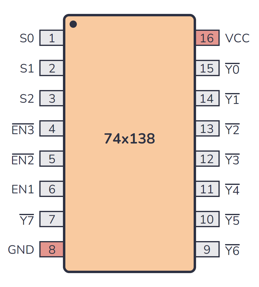
Pin Configuration and Descriptions
The 74LS138 comes in a 16-pin package. Below is the pinout and description:
| Pin No. | Pin Name | Description |
|---|---|---|
| 1 | G1 | Enable Input (Active High) |
| 2 | G2A | Enable Input (Active Low) |
| 3 | G2B | Enable Input (Active Low) |
| 4 | A | Input A (LSB of the 3-bit binary input) |
| 5 | B | Input B |
| 6 | C | Input C (MSB of the 3-bit binary input) |
| 7 | Y7 | Output 7 (Active Low) |
| 8 | GND | Ground |
| 9 | Y6 | Output 6 (Active Low) |
| 10 | Y5 | Output 5 (Active Low) |
| 11 | Y4 | Output 4 (Active Low) |
| 12 | Y3 | Output 3 (Active Low) |
| 13 | Y2 | Output 2 (Active Low) |
| 14 | Y1 | Output 1 (Active Low) |
| 15 | Y0 | Output 0 (Active Low) |
| 16 | Vcc | Supply Voltage |
Usage Instructions
How to Use the 74LS138 in a Circuit
- Power Supply: Connect the Vcc pin (Pin 16) to a 5V power supply and the GND pin (Pin 8) to ground.
- Enable Inputs:
- The decoder is enabled when G1 (Pin 1) is HIGH and both G2A (Pin 2) and G2B (Pin 3) are LOW.
- If the enable conditions are not met, all outputs remain HIGH (inactive).
- Input Selection: Provide a 3-bit binary input using pins A (Pin 4), B (Pin 5), and C (Pin 6). The binary value determines which output is activated.
- Outputs: The corresponding output pin (Y0 to Y7) will go LOW based on the binary input, while all other outputs remain HIGH.
Example Circuit
Below is an example of how to connect the 74LS138 to an Arduino UNO for address decoding:
Circuit Connections
- Connect Vcc (Pin 16) to the Arduino's 5V pin.
- Connect GND (Pin 8) to the Arduino's GND pin.
- Connect A, B, and C (Pins 4, 5, and 6) to Arduino digital pins 2, 3, and 4, respectively.
- Connect G1 (Pin 1) to Arduino digital pin 5.
- Connect G2A and G2B (Pins 2 and 3) to GND.
Arduino Code Example
// Define input pins for the 74LS138
const int pinA = 2;  // Connects to A (Pin 4)
const int pinB = 3;  // Connects to B (Pin 5)
const int pinC = 4;  // Connects to C (Pin 6)
const int enableG1 = 5;  // Connects to G1 (Pin 1)

// Binary input values to activate outputs Y0 to Y7
int binaryInputs[8][3] = {
  {0, 0, 0},  // Y0
  {1, 0, 0},  // Y1
  {0, 1, 0},  // Y2
  {1, 1, 0},  // Y3
  {0, 0, 1},  // Y4
  {1, 0, 1},  // Y5
  {0, 1, 1},  // Y6
  {1, 1, 1}   // Y7
};

void setup() {
  // Set pins as outputs
  pinMode(pinA, OUTPUT);
  pinMode(pinB, OUTPUT);
  pinMode(pinC, OUTPUT);
  pinMode(enableG1, OUTPUT);

  // Enable the decoder
  digitalWrite(enableG1, HIGH);  // G1 is active HIGH
}

void loop() {
  for (int i = 0; i < 8; i++) {
    // Set binary inputs
    digitalWrite(pinA, binaryInputs[i][0]);
    digitalWrite(pinB, binaryInputs[i][1]);
    digitalWrite(pinC, binaryInputs[i][2]);

    // Wait for 1 second before switching to the next output
    delay(1000);
  }
}
Important Considerations
- Ensure that the enable inputs (G1, G2A, and G2B) are properly configured to avoid unexpected behavior.
- Use pull-up or pull-down resistors on unused inputs to prevent floating states.
- Avoid exceeding the maximum voltage and current ratings to prevent damage to the component.
Troubleshooting and FAQs
Common Issues and Solutions
No Output Activation:
- Verify that G1 is HIGH and both G2A and G2B are LOW.
- Check the power supply connections to Vcc and GND.
- Ensure that the input pins (A, B, and C) are receiving the correct binary signals.
Multiple Outputs Activated:
- Check for noise or interference on the input lines.
- Ensure that only one binary combination is applied to the inputs at a time.
Outputs Not Responding to Inputs:
- Confirm that the input voltage levels meet the required thresholds (HIGH ≥ 2V, LOW ≤ 0.8V).
- Inspect the circuit for loose or incorrect connections.
FAQs
Q1: Can the 74LS138 be used with a 3.3V microcontroller?
A1: The 74LS138 is designed for a 5V supply. While it may work with 3.3V logic inputs in some cases, it is not guaranteed. Use a level shifter if interfacing with a 3.3V microcontroller.
Q2: What happens if all enable inputs are inactive?
A2: If G1 is LOW or either G2A or G2B is HIGH, all outputs will remain HIGH (inactive).
Q3: Can multiple 74LS138 chips be cascaded?
A3: Yes, multiple 74LS138 chips can be cascaded to decode larger address spaces by using the enable inputs for hierarchical control.
Q4: Are the outputs of the 74LS138 open-collector?
A4: No, the outputs are not open-collector. They are active-low outputs with standard TTL drive capability.