
How to Use ATmega168-20PU: Examples, Pinouts, and Specs
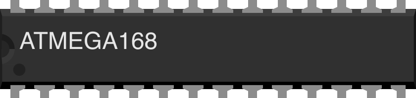
 Design with ATmega168-20PU in Cirkit Designer
Introduction
The ATmega168-20PU is a low-power 8-bit microcontroller developed by Microchip Technology (formerly Atmel). It is based on the AVR RISC architecture and is designed for high-performance and efficient operation in embedded systems. With 16KB of flash memory, 1KB of SRAM, and 512 bytes of EEPROM, the ATmega168-20PU is well-suited for a wide range of applications, including consumer electronics, industrial automation, and IoT devices.
Explore Projects Built with ATmega168-20PU
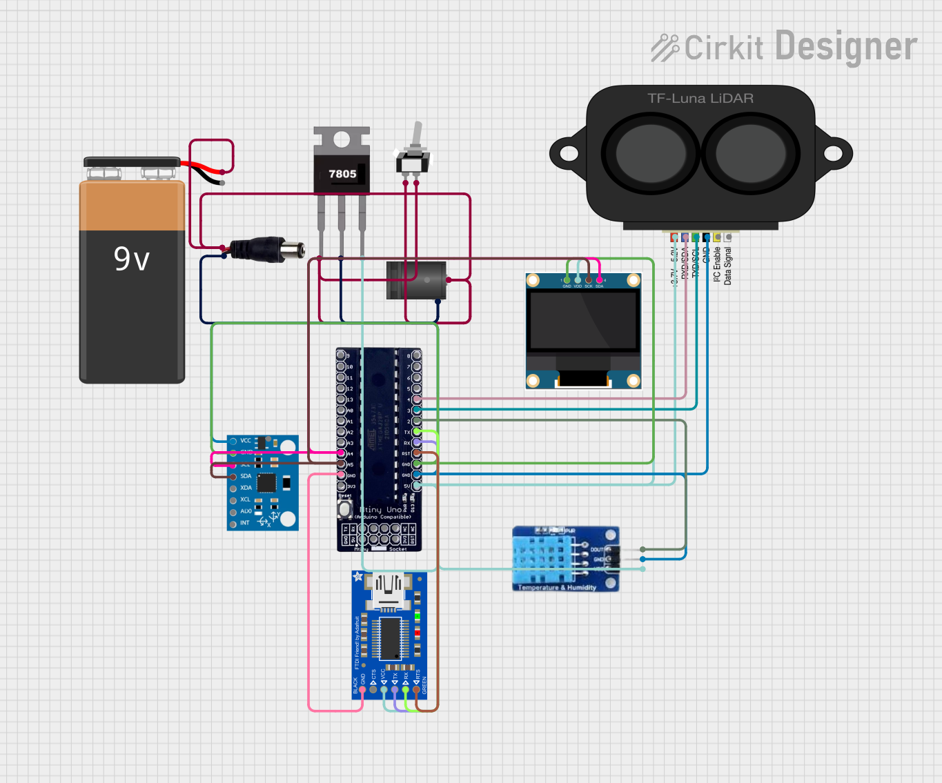 Open Project in Cirkit Designer
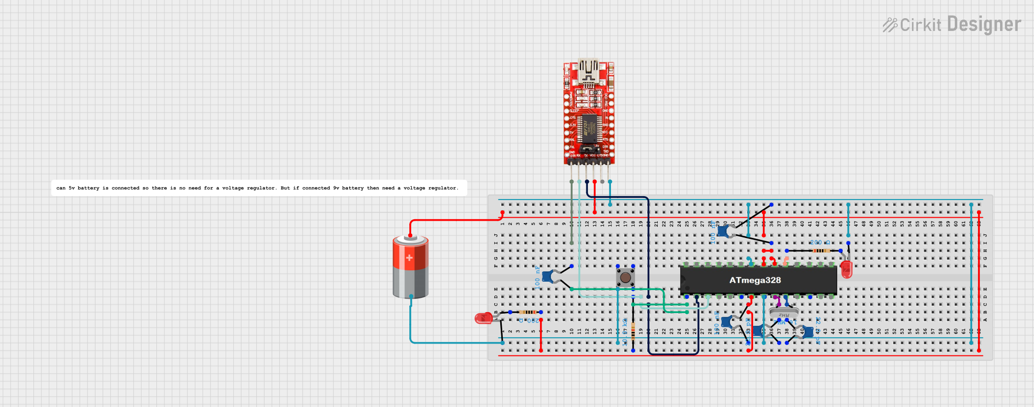 Open Project in Cirkit Designer
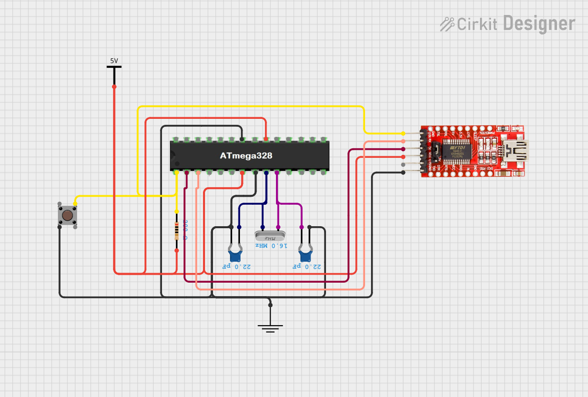 Open Project in Cirkit Designer
 Open Project in Cirkit Designer
Explore Projects Built with ATmega168-20PU
Open Project in Cirkit DesignerOpen Project in Cirkit DesignerOpen Project in Cirkit DesignerOpen Project in Cirkit DesignerCommon Applications and Use Cases
- Embedded systems and prototyping
- Home automation and IoT devices
- Robotics and motor control
- Data acquisition and sensor interfacing
- Educational projects and Arduino-based designs
Technical Specifications
The ATmega168-20PU offers a robust set of features and capabilities. Below are its key technical specifications:
| Parameter | Value |
|---|---|
| Architecture | 8-bit AVR RISC |
| Operating Voltage | 2.7V to 5.5V |
| Maximum Clock Frequency | 20 MHz |
| Flash Memory | 16KB |
| SRAM | 1KB |
| EEPROM | 512 bytes |
| General-Purpose I/O Pins | 23 |
| Timers | Two 8-bit, One 16-bit |
| ADC | 10-bit, 6 channels |
| Communication Interfaces | USART, SPI, I2C (TWI) |
| Power Consumption (Active) | ~1.2 mA at 1 MHz, 3V |
| Package Type | 28-pin DIP |
Pin Configuration and Descriptions
The ATmega168-20PU comes in a 28-pin Dual Inline Package (DIP). Below is the pinout and description:
| Pin Number | Pin Name | Description |
|---|---|---|
| 1 | PC6 (RESET) | Reset input (active low) |
| 2 | PD0 (RXD) | USART Receive Data |
| 3 | PD1 (TXD) | USART Transmit Data |
| 4 | PD2 | External Interrupt 0 |
| 5 | PD3 | External Interrupt 1 / PWM Output |
| 6 | PD4 | I/O Pin |
| 7 | VCC | Supply Voltage |
| 8 | GND | Ground |
| 9 | PB6 | Crystal Oscillator Input |
| 10 | PB7 | Crystal Oscillator Output |
| 11 | PD5 | PWM Output / I/O Pin |
| 12 | PD6 | PWM Output / I/O Pin |
| 13 | PD7 | I/O Pin |
| 14 | PB0 | I/O Pin |
| 15 | PB1 | PWM Output / I/O Pin |
| 16 | PB2 | SPI Chip Select |
| 17 | PB3 | SPI MOSI |
| 18 | PB4 | SPI MISO |
| 19 | PB5 | SPI SCK |
| 20 | AVCC | Analog Supply Voltage |
| 21 | AREF | Analog Reference Voltage |
| 22 | GND | Ground |
| 23 | PC0 | ADC Channel 0 |
| 24 | PC1 | ADC Channel 1 |
| 25 | PC2 | ADC Channel 2 |
| 26 | PC3 | ADC Channel 3 |
| 27 | PC4 (SDA) | ADC Channel 4 / I2C Data Line |
| 28 | PC5 (SCL) | ADC Channel 5 / I2C Clock Line |
Usage Instructions
The ATmega168-20PU is versatile and can be used in a variety of circuits. Below are the steps and considerations for using this microcontroller:
Basic Circuit Setup
- Power Supply: Connect the VCC pin to a 5V power source and the GND pin to ground. For analog operations, connect AVCC to the same voltage as VCC and AREF to the desired reference voltage.
- Reset Pin: Connect a 10kΩ pull-up resistor to the RESET pin to ensure proper operation.
- Clock Source: Use an external 16 MHz crystal oscillator connected to PB6 and PB7, along with two 22pF capacitors to ground.
- I/O Pins: Configure the I/O pins as input or output in the software, depending on your application.
Programming the Microcontroller
The ATmega168-20PU can be programmed using an ISP (In-System Programmer) or an Arduino as an ISP. The microcontroller is also compatible with the Arduino IDE when used with the appropriate bootloader.
Example: Blinking an LED with Arduino UNO
The ATmega168-20PU can be used with an Arduino UNO board. Below is an example code to blink an LED connected to pin PB0:
// Blink an LED connected to PB0 (Pin 14 on ATmega168-20PU)

// Define the pin number for the LED
#define LED_PIN 8  // PB0 corresponds to digital pin 8 on Arduino

void setup() {
  pinMode(LED_PIN, OUTPUT);  // Set LED_PIN as an output
}

void loop() {
  digitalWrite(LED_PIN, HIGH);  // Turn the LED on
  delay(1000);                  // Wait for 1 second
  digitalWrite(LED_PIN, LOW);   // Turn the LED off
  delay(1000);                  // Wait for 1 second
}
Best Practices
- Use decoupling capacitors (e.g., 0.1µF) near the VCC and AVCC pins to reduce noise.
- Avoid leaving unused pins floating; configure them as inputs with pull-up resistors or as outputs.
- Ensure proper grounding to minimize noise and interference in analog applications.
Troubleshooting and FAQs
Common Issues
Microcontroller Not Responding
- Ensure the power supply voltage is within the operating range (2.7V to 5.5V).
- Verify the RESET pin is connected to a pull-up resistor.
- Check the clock source (crystal oscillator or external clock) for proper connections.
Incorrect ADC Readings
- Ensure AVCC is connected to the same voltage as VCC.
- Use a stable reference voltage on the AREF pin.
- Avoid noise on analog input pins by using proper shielding and grounding.
Programming Errors
- Verify the ISP connections and ensure the programmer is compatible.
- Check the fuse settings if using a custom clock source.
FAQs
Q: Can the ATmega168-20PU be used with the Arduino IDE?
A: Yes, the ATmega168-20PU is compatible with the Arduino IDE when flashed with the appropriate bootloader.
Q: What is the maximum clock speed of the ATmega168-20PU?
A: The maximum clock speed is 20 MHz when operating at 5V.
Q: How many PWM channels are available?
A: The ATmega168-20PU has six PWM channels.
Q: Can I use the ATmega168-20PU for battery-powered applications?
A: Yes, its low-power consumption makes it suitable for battery-powered devices. Use sleep modes to further reduce power usage.
By following the guidelines and best practices outlined in this documentation, you can effectively integrate the ATmega168-20PU into your projects.