How to Use ADS1299 breakout: Examples, Pinouts, and Specs
Introduction
The ADS1299 breakout is a development board built around the Texas Instruments ADS1299, a high-performance, low-power, 24-bit analog-to-digital converter (ADC). This component is specifically designed for biopotential measurements, such as electrocardiography (ECG) and electroencephalography (EEG). It offers multiple channels for simultaneous data acquisition, making it ideal for medical, research, and wearable applications.
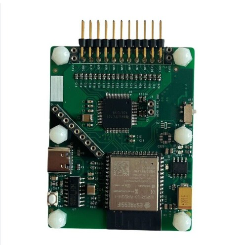
Explore Projects Built with ADS1299 breakout
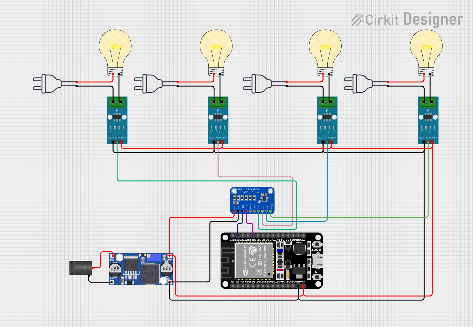
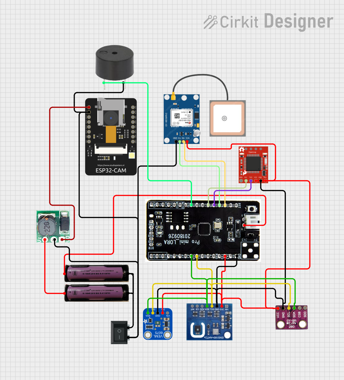
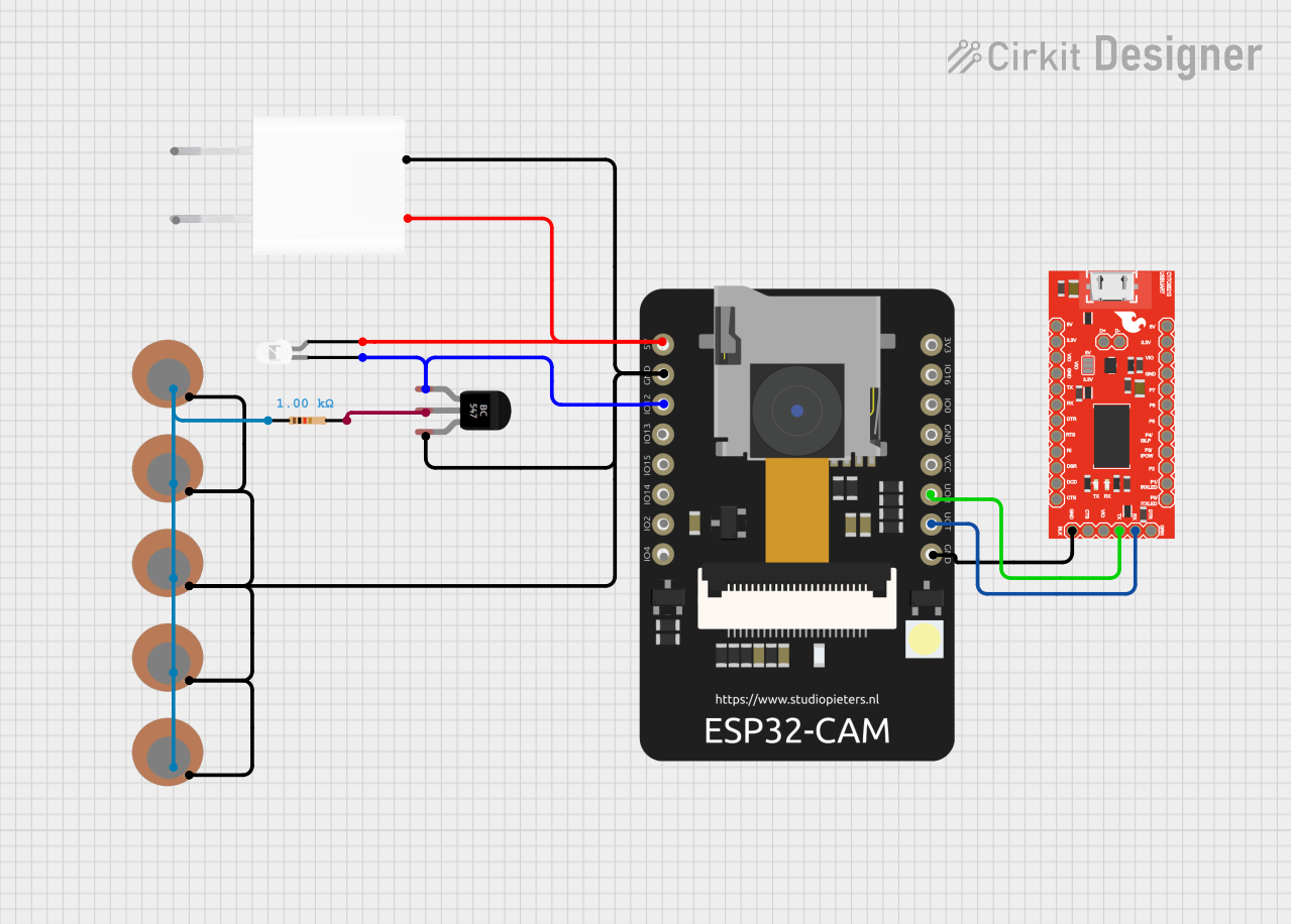
Explore Projects Built with ADS1299 breakout
Common Applications and Use Cases
- EEG (Electroencephalography) systems for brain activity monitoring
- ECG (Electrocardiography) systems for heart monitoring
- EMG (Electromyography) systems for muscle activity analysis
- Wearable health monitoring devices
- Research and development in biomedical signal processing
Technical Specifications
The ADS1299 breakout board provides access to the full functionality of the ADS1299 IC. Below are the key technical specifications:
Key Features
- Resolution: 24-bit ADC
- Number of Channels: 8 differential input channels
- Input Voltage Range: ±4.5 V (with ±5 V supplies)
- Programmable Gain Amplifiers (PGA): Gains of 1, 2, 4, 6, 8, 12, and 24
- Sampling Rate: Up to 16 kSPS (kilosamples per second)
- Power Supply: ±2.5 V analog, 3.3 V digital
- Integrated Features: Built-in reference voltage, lead-off detection, and bias drive
- Interface: SPI (Serial Peripheral Interface)
- Power Consumption: 0.85 mW/channel at 250 SPS
Pin Configuration and Descriptions
The breakout board exposes the ADS1299 pins for easy integration into your circuit. Below is the pin configuration:
| Pin Name | Type | Description |
|---|---|---|
| VDD | Power Input | Digital power supply (3.3 V). |
| AVDD | Power Input | Analog positive power supply (+2.5 V). |
| AVSS | Power Input | Analog negative power supply (-2.5 V). |
| GND | Ground | Ground reference for the circuit. |
| CS | Digital Input | Chip select for SPI communication. Active low. |
| SCLK | Digital Input | SPI clock input. |
| DIN | Digital Input | SPI data input (Master Out Slave In - MOSI). |
| DOUT | Digital Output | SPI data output (Master In Slave Out - MISO). |
| DRDY | Digital Output | Data ready signal. Indicates when new data is available. |
| RESET | Digital Input | Resets the ADS1299. Active low. |
| START | Digital Input | Starts or stops conversions. Active high. |
| CLKSEL | Digital Input | Selects the clock source (internal or external). |
| BIASOUT | Analog Output | Bias drive output for patient reference electrode. |
| IN1P - IN8P | Analog Input | Positive differential input for channels 1 to 8. |
| IN1N - IN8N | Analog Input | Negative differential input for channels 1 to 8. |
Usage Instructions
How to Use the ADS1299 Breakout in a Circuit
- Power Supply: Connect the analog power supplies (AVDD and AVSS) to ±2.5 V and the digital power supply (VDD) to 3.3 V. Ensure all grounds (GND) are connected.
- SPI Communication: Connect the SPI pins (CS, SCLK, DIN, DOUT) to your microcontroller or development board. Configure the SPI interface for the ADS1299 (Mode 1: CPOL = 0, CPHA = 1).
- Input Signals: Connect the biopotential electrodes to the differential input pins (INxP and INxN). Use the BIASOUT pin for the reference electrode.
- Clock Source: Use the CLKSEL pin to select the clock source. For internal clock, tie CLKSEL to GND.
- Start Conversions: Use the START pin to begin data acquisition. Monitor the DRDY pin to know when new data is available.
Important Considerations and Best Practices
- Electrode Placement: Ensure proper placement of electrodes for accurate biopotential measurements.
- Noise Reduction: Use shielded cables and proper grounding to minimize noise in the signals.
- Bias Drive: Use the BIASOUT pin to drive the reference electrode for improved common-mode noise rejection.
- Power Supply Decoupling: Add decoupling capacitors (e.g., 0.1 µF and 10 µF) close to the power supply pins to reduce noise.
- SPI Configuration: Ensure the SPI clock speed does not exceed the ADS1299's maximum supported rate.
Example Code for Arduino UNO
Below is an example of how to interface the ADS1299 breakout with an Arduino UNO using SPI:
#include <SPI.h>

// Pin definitions
#define CS_PIN 10  // Chip select pin
#define DRDY_PIN 9 // Data ready pin
#define RESET_PIN 8 // Reset pin

void setup() {
  // Initialize serial communication
  Serial.begin(115200);

  // Configure SPI
  SPI.begin();
  SPI.setDataMode(SPI_MODE1); // CPOL = 0, CPHA = 1
  SPI.setClockDivider(SPI_CLOCK_DIV16); // Adjust as needed for your setup

  // Configure pins
  pinMode(CS_PIN, OUTPUT);
  pinMode(DRDY_PIN, INPUT);
  pinMode(RESET_PIN, OUTPUT);

  // Reset the ADS1299
  digitalWrite(RESET_PIN, LOW);
  delay(10); // Hold reset low for 10 ms
  digitalWrite(RESET_PIN, HIGH);

  // Initialize ADS1299
  digitalWrite(CS_PIN, LOW);
  SPI.transfer(0x11); // Example: Send a command to read the ID register
  byte id = SPI.transfer(0x00); // Read the response
  digitalWrite(CS_PIN, HIGH);

  Serial.print("ADS1299 ID: 0x");
  Serial.println(id, HEX);
}

void loop() {
  // Wait for data ready signal
  if (digitalRead(DRDY_PIN) == LOW) {
    digitalWrite(CS_PIN, LOW);
    // Example: Read data from the ADS1299
    for (int i = 0; i < 9; i++) { // 8 channels + status byte
      byte data = SPI.transfer(0x00);
      Serial.print(data, HEX);
      Serial.print(" ");
    }
    Serial.println();
    digitalWrite(CS_PIN, HIGH);
  }
}
Troubleshooting and FAQs
Common Issues and Solutions
No Data Output:
- Ensure the SPI connections are correct and the SPI mode is set to Mode 1.
- Verify that the START pin is high to enable conversions.
High Noise in Signals:
- Check the electrode connections and ensure proper placement.
- Use shielded cables and minimize external interference.
ADS1299 Not Responding:
- Verify the power supply voltages and connections.
- Ensure the RESET pin is toggled low and then high during initialization.
Incorrect Data:
- Confirm the SPI clock speed is within the ADS1299's specifications.
- Check the gain settings and input voltage range.
FAQs
Q: Can I use the ADS1299 breakout with a 5 V microcontroller?
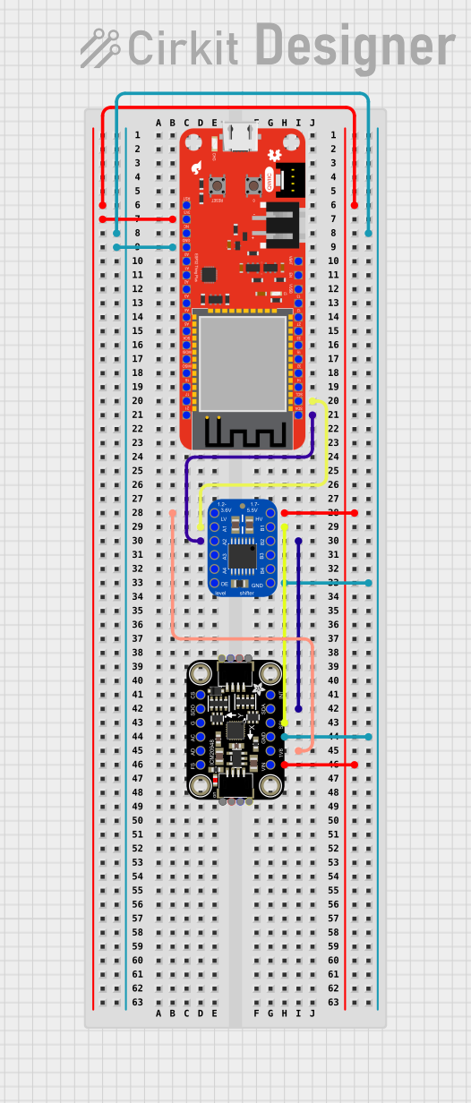
A: No, the ADS1299 operates at 3.3 V logic levels. Use a level shifter if interfacing with a 5 V microcontroller.
Q: What is the maximum sampling rate of the ADS1299?
A: The ADS1299 supports a maximum sampling rate of 16 kSPS.
Q: How do I reduce common-mode noise in my measurements?
A: Use the BIASOUT pin to drive the reference electrode and ensure proper grounding.
Q: Can I use fewer than 8 channels?
A: Yes, unused channels can be powered down to save power.
This documentation provides a comprehensive guide to using the ADS1299 breakout for biopotential measurements. For further details, refer to the Texas Instruments ADS1299 datasheet.