How to Use LTC2664: Examples, Pinouts, and Specs
Introduction
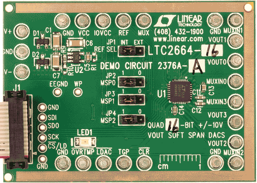
The LTC2664, manufactured by Linear Technology, is a high-precision 16-bit digital-to-analog converter (DAC) designed for applications requiring accurate and low-noise analog signal generation. It features a versatile serial interface, making it easy to integrate into digital systems. The LTC2664 is ideal for use in industrial control systems, instrumentation, data acquisition, and other applications where precise analog output is critical.
Explore Projects Built with LTC2664
Explore Projects Built with LTC2664
Common Applications:
- Industrial process control
- Precision instrumentation
- Data acquisition systems
- Signal generation
- Automated test equipment (ATE)
Technical Specifications
The LTC2664 offers robust performance and flexibility. Below are its key technical specifications:
| Parameter | Value |
|---|---|
| Resolution | 16 bits |
| Output Voltage Range | 0V to 5V, 0V to 10V, ±5V, ±10V (configurable) |
| Output Current Drive | ±10mA |
| Power Supply Voltage | 2.7V to 5.5V (VDD) |
| Reference Voltage | Internal or External (2.5V internal ref) |
| Interface | SPI-compatible serial interface |
| Settling Time | 10µs (typical) |
| Integral Nonlinearity (INL) | ±4 LSB (max) |
| Differential Nonlinearity | ±1 LSB (max) |
| Operating Temperature Range | -40°C to 125°C |
Pin Configuration and Descriptions
The LTC2664 is available in a compact package with the following pin configuration:
| Pin Number | Pin Name | Description |
|---|---|---|
| 1 | VDD | Positive power supply (2.7V to 5.5V). |
| 2 | GND | Ground reference. |
| 3 | SCK | Serial clock input for SPI communication. |
| 4 | SDI | Serial data input for SPI communication. |
| 5 | CS/LD | Chip select (active low) and load control. |
| 6 | SDO | Serial data output for daisy-chaining multiple devices. |
| 7 | REF | Reference voltage input/output (internal 2.5V or external reference). |
| 8-11 | DACx_OUT | Analog output pins for DAC channels (DAC0_OUT, DAC1_OUT, DAC2_OUT, DAC3_OUT). |
Usage Instructions
How to Use the LTC2664 in a Circuit
- Power Supply: Connect the VDD pin to a stable power supply (2.7V to 5.5V) and the GND pin to the ground.
- Reference Voltage: Use the internal 2.5V reference or connect an external reference voltage to the REF pin.
- SPI Communication:
- Connect the SCK, SDI, and CS/LD pins to the SPI interface of your microcontroller or processor.
- If daisy-chaining multiple LTC2664 devices, connect the SDO pin of one device to the SDI pin of the next.
- Analog Outputs: Connect the DACx_OUT pins to the desired load or circuit. Ensure the load does not exceed the ±10mA drive capability.
- Programming the DAC: Use SPI commands to set the desired output voltage for each DAC channel.
Important Considerations and Best Practices
- Bypass Capacitors: Place a 0.1µF ceramic capacitor close to the VDD pin to reduce power supply noise.
- Load Impedance: Ensure the load impedance is high enough to avoid excessive current draw from the DAC outputs.
- SPI Timing: Follow the SPI timing requirements specified in the datasheet to ensure reliable communication.
- Thermal Management: Operate the device within the specified temperature range to maintain accuracy and reliability.
Example Code for Arduino UNO
Below is an example of how to interface the LTC2664 with an Arduino UNO using SPI:
#include <SPI.h>

// Define SPI pins for LTC2664
const int CS_PIN = 10; // Chip Select pin connected to LTC2664 CS/LD

void setup() {
  // Initialize SPI communication
  SPI.begin();
  SPI.setClockDivider(SPI_CLOCK_DIV16); // Set SPI clock speed
  SPI.setDataMode(SPI_MODE0);           // SPI mode 0
  pinMode(CS_PIN, OUTPUT);
  digitalWrite(CS_PIN, HIGH);           // Set CS pin high (inactive)
}

void loop() {
  // Example: Set DAC channel 0 to output 2.5V
  uint16_t dacValue = 32768; // 2.5V corresponds to mid-scale for 16-bit DAC
  writeToDAC(0, dacValue);   // Write to DAC channel 0
  delay(1000);               // Wait for 1 second
}

// Function to write data to LTC2664
void writeToDAC(uint8_t channel, uint16_t value) {
  uint16_t command = 0x3000 | (channel << 12); // Command to write to DAC
  uint16_t data = value;                       // 16-bit DAC value

  digitalWrite(CS_PIN, LOW);                   // Select LTC2664
  SPI.transfer16(command);                     // Send command and channel
  SPI.transfer16(data);                        // Send DAC value
  digitalWrite(CS_PIN, HIGH);                  // Deselect LTC2664
}
Troubleshooting and FAQs
Common Issues and Solutions
No Output Voltage:
- Verify that the power supply (VDD) and ground (GND) connections are correct.
- Ensure the SPI communication is configured correctly (clock speed, mode, etc.).
- Check that the DAC channel is properly addressed in the SPI command.
Incorrect Output Voltage:
- Confirm that the reference voltage (internal or external) is stable and accurate.
- Verify the DAC value being sent matches the desired output voltage.
Noise on Output:
- Add bypass capacitors near the power supply and reference voltage pins.
- Minimize noise on the SPI lines by using proper grounding and shielding techniques.
Device Overheating:
- Ensure the load connected to the DAC outputs does not exceed the ±10mA drive capability.
- Operate the device within the specified temperature range.
FAQs
Q: Can I use the LTC2664 with a 3.3V microcontroller?
A: Yes, the LTC2664 operates with a power supply range of 2.7V to 5.5V, making it compatible with 3.3V systems.
Q: How many LTC2664 devices can I daisy-chain?
A: The number of devices you can daisy-chain depends on the SPI clock speed and the timing requirements of your system. Refer to the datasheet for detailed timing information.
Q: Can I use an external reference voltage?
A: Yes, the LTC2664 supports both internal and external reference voltages. Connect your external reference to the REF pin.
Q: What happens if the load exceeds the current drive capability?
A: Exceeding the ±10mA drive capability may result in output voltage errors or damage to the device. Always ensure the load is within the specified limits.