How to Use CD4011 Quad Input NAND Gate IC: Examples, Pinouts, and Specs
Introduction
The CD4011 is a digital logic integrated circuit (IC) that contains four independent NAND gates, each with two inputs. It is a versatile component widely used in digital electronics for implementing various logic functions. Known for its low power consumption and wide operating voltage range, the CD4011 is a popular choice in both hobbyist and professional applications.
Explore Projects Built with CD4011 Quad Input NAND Gate IC

Explore Projects Built with CD4011 Quad Input NAND Gate IC
Common Applications and Use Cases
- Logic circuit design and implementation
- Signal processing and control systems
- Oscillator circuits
- Digital switching and timing applications
- Educational projects and prototyping
Technical Specifications
The CD4011 IC is designed to operate efficiently in a variety of environments. Below are its key technical details:
| Parameter | Value |
|---|---|
| Supply Voltage (Vcc) | 3V to 15V |
| Input Voltage Range | 0V to Vcc |
| Output Voltage Range | 0V to Vcc |
| Maximum Output Current | ±10mA |
| Propagation Delay | 60ns (typical at 5V) |
| Power Dissipation | 500mW (maximum) |
| Operating Temperature | -55°C to +125°C |
| Logic Type | CMOS |
| Number of Gates | 4 (2-input NAND gates) |
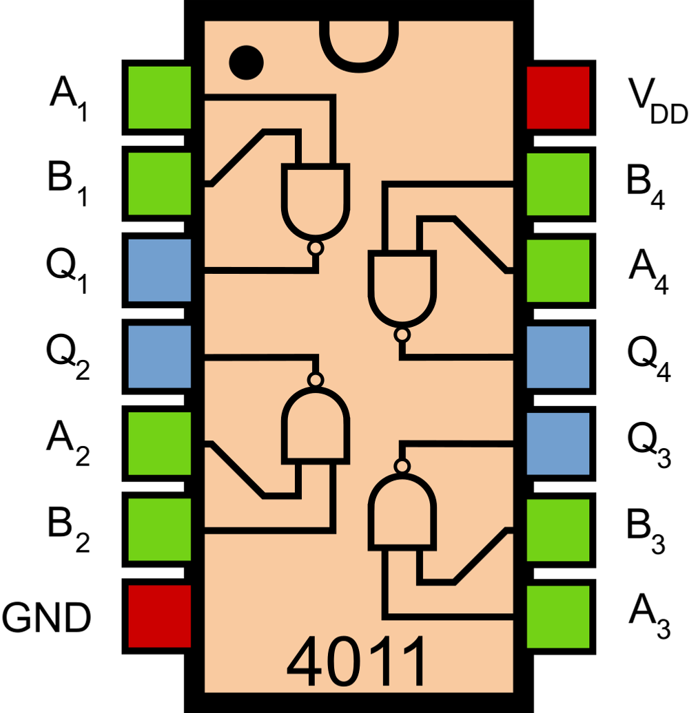
Pin Configuration and Descriptions
The CD4011 IC comes in a 14-pin Dual Inline Package (DIP). Below is the pinout and description:
| Pin Number | Pin Name | Description |
|---|---|---|
| 1 | A1 | Input 1 of NAND Gate 1 |
| 2 | B1 | Input 2 of NAND Gate 1 |
| 3 | Y1 | Output of NAND Gate 1 |
| 4 | A2 | Input 1 of NAND Gate 2 |
| 5 | B2 | Input 2 of NAND Gate 2 |
| 6 | Y2 | Output of NAND Gate 2 |
| 7 | VSS | Ground (0V) |
| 8 | Y3 | Output of NAND Gate 3 |
| 9 | A3 | Input 1 of NAND Gate 3 |
| 10 | B3 | Input 2 of NAND Gate 3 |
| 11 | Y4 | Output of NAND Gate 4 |
| 12 | A4 | Input 1 of NAND Gate 4 |
| 13 | B4 | Input 2 of NAND Gate 4 |
| 14 | VDD | Positive Supply Voltage |
Usage Instructions
How to Use the CD4011 in a Circuit
- Power Supply: Connect the VDD pin (Pin 14) to the positive supply voltage (3V to 15V) and the VSS pin (Pin 7) to ground.
- Inputs: Provide logic-level signals (0V for LOW, VDD for HIGH) to the input pins of the desired NAND gate.
- Outputs: The output pin of the NAND gate will provide the logic result based on the NAND gate truth table:
- If both inputs are HIGH, the output is LOW.
- For all other input combinations, the output is HIGH.
- Load: Ensure the output is connected to a load that does not exceed the maximum output current (±10mA).
Important Considerations and Best Practices
- Decoupling Capacitor: Place a 0.1µF ceramic capacitor close to the IC's power pins to reduce noise and stabilize the power supply.
- Unused Inputs: Connect any unused inputs to either VDD or VSS to prevent floating inputs, which can cause erratic behavior.
- Voltage Levels: Ensure that the input and output voltage levels are within the specified range to avoid damage to the IC.
- Avoid Overloading: Do not exceed the maximum output current to prevent overheating or permanent damage.
Example: Connecting CD4011 to an Arduino UNO
The CD4011 can be used with an Arduino UNO to implement basic logic functions. Below is an example of using one NAND gate to control an LED:
Circuit Connections
- Connect Pin 14 (VDD) to the Arduino's 5V pin.
- Connect Pin 7 (VSS) to the Arduino's GND pin.
- Connect two digital pins of the Arduino (e.g., D2 and D3) to Pins 1 (A1) and 2 (B1) of the CD4011.
- Connect Pin 3 (Y1) to the positive leg of an LED through a 220Ω resistor. Connect the negative leg of the LED to GND.
Arduino Code
// Define input pins for the NAND gate
const int inputA = 2; // Input A connected to Arduino pin D2
const int inputB = 3; // Input B connected to Arduino pin D3

// Define output pin for the NAND gate
const int outputY = 4; // Output Y connected to Arduino pin D4

void setup() {
  // Set input pins as outputs to control the NAND gate
  pinMode(inputA, OUTPUT);
  pinMode(inputB, OUTPUT);

  // Set output pin as input to read the NAND gate's output
  pinMode(outputY, INPUT);
}

void loop() {
  // Example logic: Toggle inputs and observe the NAND gate's output
  digitalWrite(inputA, HIGH); // Set Input A to HIGH
  digitalWrite(inputB, LOW);  // Set Input B to LOW

  // Read the output of the NAND gate
  int nandOutput = digitalRead(outputY);

  // Use the output to control an LED
  if (nandOutput == HIGH) {
    // Turn on the LED if the NAND output is HIGH
    digitalWrite(LED_BUILTIN, HIGH);
  } else {
    // Turn off the LED if the NAND output is LOW
    digitalWrite(LED_BUILTIN, LOW);
  }

  delay(1000); // Wait for 1 second before toggling inputs
}
Troubleshooting and FAQs
Common Issues and Solutions
No Output from the NAND Gate
- Cause: Incorrect power supply connections.
- Solution: Verify that VDD is connected to a positive voltage (3V to 15V) and VSS is connected to ground.
Erratic Behavior
- Cause: Floating inputs.
- Solution: Connect all unused inputs to VDD or VSS to prevent floating.
Overheating
- Cause: Exceeding the maximum output current.
- Solution: Ensure the load connected to the output does not draw more than ±10mA.
Incorrect Logic Output
- Cause: Input voltage levels are not within the specified range.
- Solution: Verify that the input signals are either 0V (LOW) or VDD (HIGH).
FAQs
Q1: Can the CD4011 operate at 3.3V?
Yes, the CD4011 can operate at a supply voltage as low as 3V, making it compatible with 3.3V systems.
Q2: What is the maximum frequency the CD4011 can handle?
The maximum operating frequency depends on the supply voltage and load conditions. At 5V, the typical propagation delay is 60ns, allowing operation up to several MHz.
Q3: Can I use the CD4011 for analog signals?
No, the CD4011 is designed for digital logic signals. Using it with analog signals may result in unpredictable behavior.