
How to Use QFN-20-0.4MM: Examples, Pinouts, and Specs
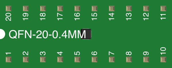
 Design with QFN-20-0.4MM in Cirkit Designer
Introduction
The QFN-20-0.4MM is a Quad Flat No-lead (QFN) package featuring 20 pins with a 0.4mm pitch. This surface-mount package is widely used in modern electronics due to its compact size, low profile, and excellent thermal and electrical performance. The QFN-20-0.4MM is ideal for applications requiring high-density board designs, such as mobile devices, IoT modules, and compact embedded systems.
Explore Projects Built with QFN-20-0.4MM
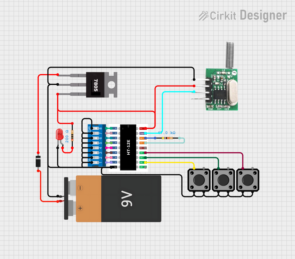 Open Project in Cirkit Designer
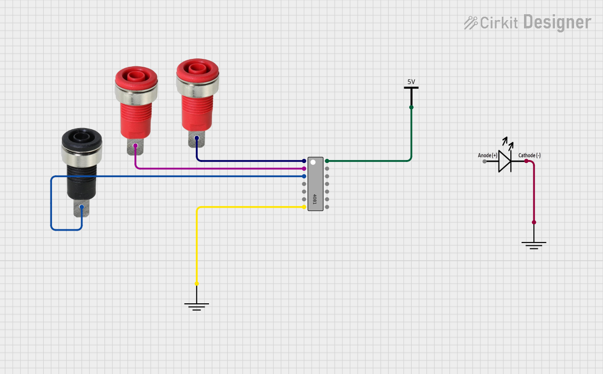 Open Project in Cirkit Designer
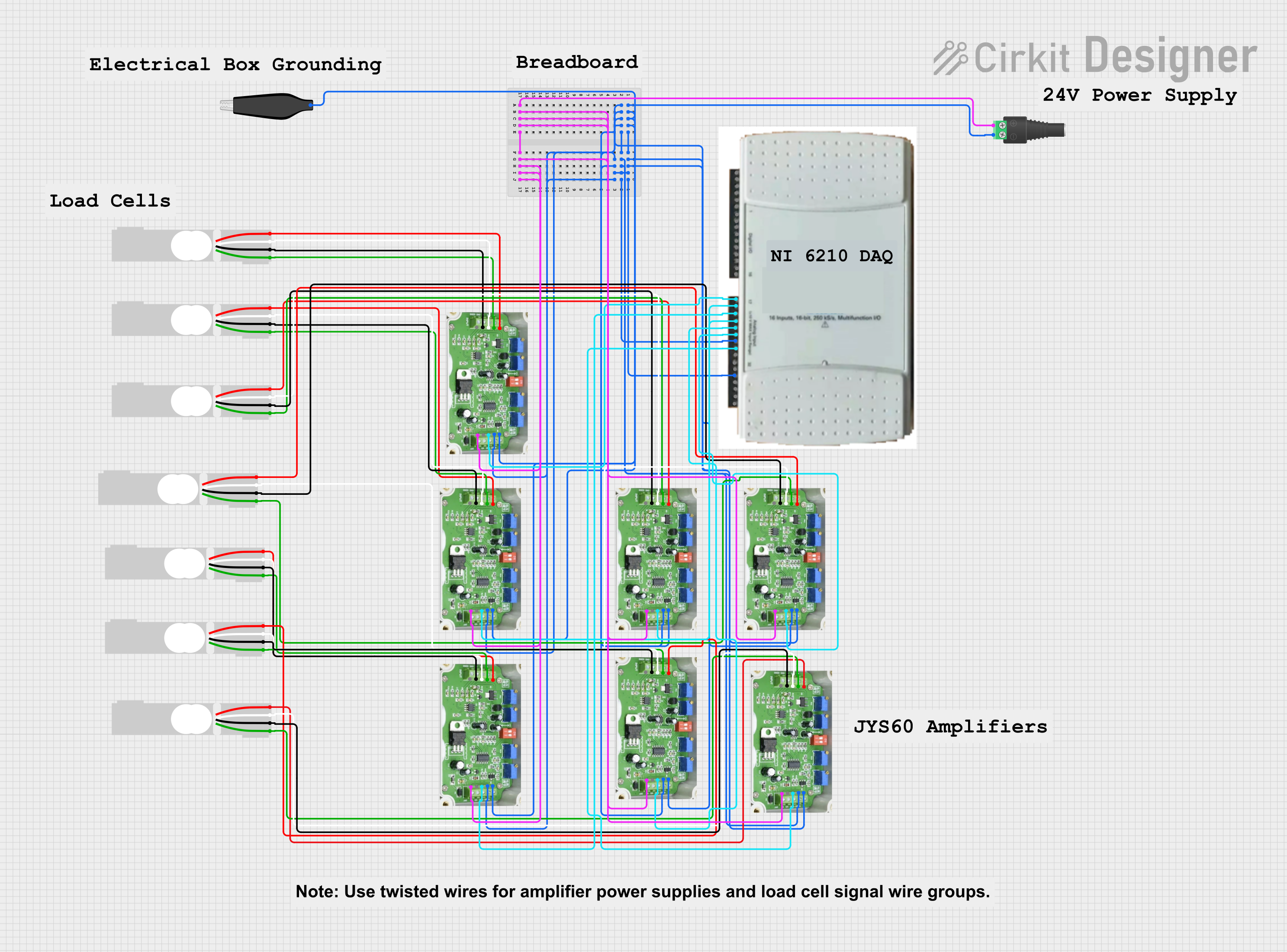 Open Project in Cirkit Designer
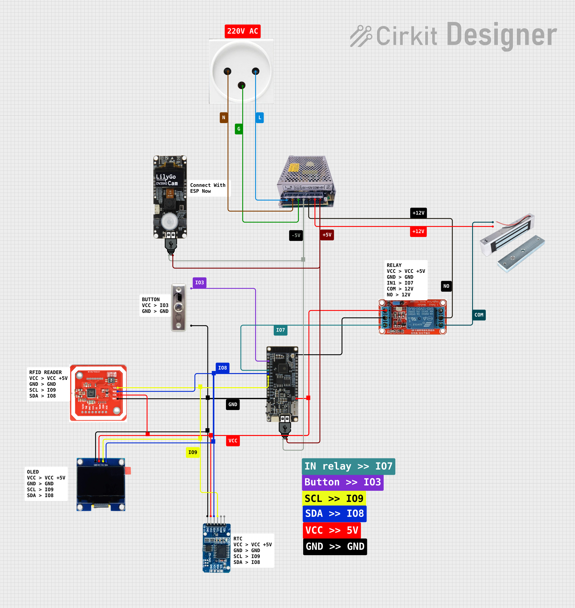 Open Project in Cirkit Designer
Explore Projects Built with QFN-20-0.4MM
Open Project in Cirkit DesignerOpen Project in Cirkit DesignerOpen Project in Cirkit DesignerOpen Project in Cirkit DesignerCommon Applications
- Mobile devices and wearables
- IoT modules and sensors
- High-frequency RF circuits
- Power management ICs
- Microcontrollers and memory devices
Technical Specifications
Key Technical Details
| Parameter | Value |
|---|---|
| Package Type | QFN (Quad Flat No-lead) |
| Pin Count | 20 |
| Pitch | 0.4mm |
| Body Size | Varies (e.g., 3mm x 3mm) |
| Thermal Pad | Yes (center pad for heat dissipation) |
| Mounting Type | Surface Mount Technology (SMT) |
| Operating Temperature | -40°C to +125°C |
| Moisture Sensitivity | Level 3 (JEDEC J-STD-020) |
Pin Configuration and Descriptions
The QFN-20-0.4MM package typically includes 20 pins arranged symmetrically around the package. The exact pinout depends on the specific IC housed in the package. Below is a generic example of pin configuration:
| Pin Number | Pin Name | Description |
|---|---|---|
| 1 | VDD | Power supply input |
| 2 | GND | Ground |
| 3-8 | GPIO1-GPIO6 | General-purpose input/output pins |
| 9 | RESET | Reset input |
| 10-15 | DATA1-DATA6 | Data or communication pins |
| 16 | CLK | Clock input |
| 17-19 | NC | No connection (reserved) |
| 20 | VSS | Ground (secondary) |
| Center Pad | Thermal Pad | Heat dissipation (connect to GND) |
Note: Always refer to the datasheet of the specific IC for the exact pinout and functionality.
Usage Instructions
How to Use the QFN-20-0.4MM in a Circuit
PCB Design Considerations:
- Ensure the PCB footprint matches the QFN-20-0.4MM dimensions, including the 0.4mm pitch.
- Include a solder mask-defined (SMD) thermal pad for proper heat dissipation.
- Use vias under the thermal pad to connect it to a ground plane for improved thermal performance.
Soldering Guidelines:
- Use reflow soldering for mounting the QFN-20-0.4MM package.
- Apply solder paste evenly on the pads, including the thermal pad.
- Follow the recommended reflow temperature profile from the IC manufacturer.
Thermal Management:
- Connect the thermal pad to a large ground plane or heat sink to dissipate heat effectively.
- Use thermal vias to improve heat transfer to other PCB layers.
Electrical Connections:
- Verify the pinout of the specific IC housed in the QFN-20-0.4MM package.
- Use decoupling capacitors near the power supply pins to reduce noise.
Example: Connecting a QFN-20-0.4MM Microcontroller to an Arduino UNO
If the QFN-20-0.4MM package houses a microcontroller, you can interface it with an Arduino UNO for testing or prototyping. Below is an example of Arduino code to communicate with a QFN-20-0.4MM microcontroller via I2C:
#include <Wire.h> // Include the Wire library for I2C communication

#define QFN_I2C_ADDRESS 0x40 // Replace with the actual I2C address of the QFN IC

void setup() {
  Wire.begin(); // Initialize I2C communication
  Serial.begin(9600); // Start serial communication for debugging
  Serial.println("Initializing QFN-20-0.4MM...");
}

void loop() {
  Wire.beginTransmission(QFN_I2C_ADDRESS); // Start communication with QFN IC
  Wire.write(0x01); // Send a command or register address (example: 0x01)
  Wire.endTransmission(); // End the transmission

  delay(100); // Wait for the IC to process the command

  Wire.requestFrom(QFN_I2C_ADDRESS, 1); // Request 1 byte of data from the IC
  if (Wire.available()) {
    int data = Wire.read(); // Read the received data
    Serial.print("Received data: ");
    Serial.println(data);
  }

  delay(1000); // Wait before sending the next command
}
Note: Replace the I2C address and commands with those specific to the IC in the QFN-20-0.4MM package.
Best Practices
- Always use the recommended PCB footprint and soldering guidelines from the IC manufacturer.
- Avoid excessive solder paste on the thermal pad to prevent bridging.
- Use X-ray inspection to verify solder joint quality, especially for the thermal pad.
Troubleshooting and FAQs
Common Issues
Poor Solder Joints:
- Cause: Insufficient or uneven solder paste application.
- Solution: Use a stencil to apply solder paste evenly. Verify reflow temperature profile.
Overheating:
- Cause: Thermal pad not properly connected to the ground plane.
- Solution: Ensure the thermal pad is soldered and connected to a heat sink or ground plane.
Electrical Noise:
- Cause: Lack of decoupling capacitors near power pins.
- Solution: Place decoupling capacitors (e.g., 0.1µF) close to the power supply pins.
Incorrect Pin Connections:
- Cause: Misinterpreting the pinout or incorrect PCB layout.
- Solution: Double-check the IC datasheet for the correct pinout and functionality.
FAQs
Q1: Can I hand-solder a QFN-20-0.4MM package?
A1: Hand-soldering is challenging due to the small pitch and lack of leads. Reflow soldering is recommended, but with proper tools (e.g., hot air station) and techniques, hand-soldering is possible.
Q2: How do I verify the soldering quality of the thermal pad?
A2: Use X-ray inspection or thermal imaging to ensure proper soldering and heat dissipation.
Q3: What is the purpose of the thermal pad?
A3: The thermal pad improves heat dissipation and enhances the electrical grounding of the IC.
Q4: Can I use the QFN-20-0.4MM package for high-frequency applications?
A4: Yes, the QFN package is well-suited for high-frequency applications due to its low inductance and excellent thermal performance.